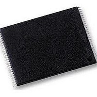
S29GL032N90TFI030 Spansion Inc., S29GL032N90TFI030 Datasheet - Page 60

S29GL032N90TFI030
Manufacturer Part Number
S29GL032N90TFI030
Description
Flash 3V 32Mb Float Gate two address 90s
Manufacturer
Spansion Inc.
Datasheet
1.S29GL032N90TFI010.pdf
(81 pages)
Specifications of S29GL032N90TFI030
Memory Type
NOR
Memory Size
32 Mbit
Access Time
90 ns
Data Bus Width
8 bit, 16 bit
Architecture
Uniform / Boot Sector
Interface Type
Page-mode
Supply Voltage (max)
3.6 V
Supply Voltage (min)
2.7 V
Maximum Operating Current
50 mA
Mounting Style
SMD/SMT
Operating Temperature
+ 85 C
Package / Case
TSOP-48
Ic Interface Type
CFI, Parallel
Supply Voltage Range
2.7V To 3.6V
Memory Case Style
TSOP
No. Of Pins
48
Lead Free Status / RoHS Status
Lead free / RoHS Compliant
Lead Free Status / RoHS Status
Lead free / RoHS Compliant, Lead free / RoHS Compliant
Available stocks
Company
Part Number
Manufacturer
Quantity
Price
Company:
Part Number:
S29GL032N90TFI030
Manufacturer:
SPANSION
Quantity:
6 035
Part Number:
S29GL032N90TFI030
Manufacturer:
SPANSION
Quantity:
20 000
Company:
Part Number:
S29GL032N90TFI030
Manufacturer:
SPANSIO
Quantity:
3 888
Company:
Part Number:
S29GL032N90TFI030H
Manufacturer:
Spansion
Quantity:
1 440
Part Number:
S29GL032N90TFI030H
Manufacturer:
SPANSION
Quantity:
20 000
10.18 DQ1: Write-to-Buffer Abort
Notes
1. DQ5 switches to 1 when an Embedded Program, Embedded Erase, or Write-to-Buffer operation exceeded the maximum timing limits. Refer to the section on
2. DQ7 and DQ2 require a valid address when reading status information. Refer to the appropriate subsection for further details.
3. The Data# Polling algorithm should be used to monitor the last loaded write-buffer address location.
4. DQ1 switches to 1 when the device aborts the write-to-buffer operation.
60
Standard Mode
Program Suspend Mode
Erase Suspend Mode
Write-to-
Buffer
DQ5 for more information.
DQ1 indicates whether a Write-to-Buffer operation was aborted. Under these conditions DQ1 produces a 1.
The system must issue the Write-to-Buffer-Abort-Reset command sequence to return the device to reading
array data. See
Embedded Program Algorithm
Embedded Erase Algorithm
Program-
Suspend
Read
Erase-
Suspend
Read
Erase-Suspend-Program
(Embedded Program)
Busy
Abort
Status
(Note 3)
(Note 4)
Write Buffer on page 18
Program-Suspended
Sector
Non-Program
Suspended Sector
Erase-Suspended Sector
Non-Erase Suspended
Sector
Table 10.5 Write Operation Status
S29GL-N MirrorBit
for more details.
(Note 2)
D a t a
DQ7#
DQ7#
DQ7#
DQ7#
DQ7
®
0
1
Flash Family
No toggle
S h e e t
Toggle
Toggle
Toggle
Toggle
Toggle
DQ6
Invalid (not allowed)
(Note 1)
DQ5
Data
Data
0
0
0
0
0
0
S29GL-N_01_12 October 29, 2008
DQ3
N/A
N/A
N/A
N/A
N/A
1
No toggle
(Note 2)
Toggle
Toggle
DQ2
N/A
N/A
N/A
DQ1
N/A
N/A
N/A
0
0
1
RY/BY#
0
0
1
1
1
1
0
0
0


