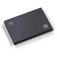
LCMXO640C-3TN100C Lattice, LCMXO640C-3TN100C Datasheet - Page 17

LCMXO640C-3TN100C
Manufacturer Part Number
LCMXO640C-3TN100C
Description
CPLD - Complex Programmable Logic Devices 640 LUTS 74 I/O
Manufacturer
Lattice
Series
MachXOr
Datasheet
1.LCMXO640C-3TN100C.pdf
(95 pages)
Specifications of LCMXO640C-3TN100C
Memory Type
SRAM
Number Of Macrocells
320
Delay Time
4.9 ns
Number Of Programmable I/os
74
Operating Supply Voltage
1.8 V, 2.5 V, 3.3 V
Supply Current
17 mA
Maximum Operating Temperature
+ 90 C
Minimum Operating Temperature
0 C
Package / Case
TQFP-100
Mounting Style
SMD/SMT
Supply Voltage (max)
3.465 V
Supply Voltage (min)
1.71 V
Programmable Type
In System Programmable
Delay Time Tpd(1) Max
4.9ns
Voltage Supply - Internal
1.71 V ~ 3.465 V
Number Of Logic Elements/blocks
-
Number Of Gates
-
Number Of I /o
74
Operating Temperature
0°C ~ 85°C
Mounting Type
*
Lead Free Status / RoHS Status
Lead free / RoHS Compliant
Available stocks
Company
Part Number
Manufacturer
Quantity
Price
Company:
Part Number:
LCMXO640C-3TN100C
Manufacturer:
STC
Quantity:
12 000
Company:
Part Number:
LCMXO640C-3TN100C
Manufacturer:
Lattice Semiconductor Corporation
Quantity:
10 000
Part Number:
LCMXO640C-3TN100C
Manufacturer:
LATTICE
Quantity:
20 000
Lattice Semiconductor
PIO Groups
On the MachXO devices, PIO cells are assembled into two different types of PIO groups, those with four PIO cells
and those with six PIO cells. PIO groups with four IOs are placed on the left and right sides of the device while PIO
groups with six IOs are placed on the top and bottom. The individual PIO cells are connected to their respective
sysIO buffers and PADs.
On all MachXO devices, two adjacent PIOs can be joined to provide a complementary Output driver pair. The I/O
pin pairs are labeled as "T" and "C" to distinguish between the true and complement pins.
The MachXO1200 and MachXO2280 devices contain enhanced I/O capability. All PIO pairs on these larger
devices can implement differential receivers. In addition, half of the PIO pairs on the left and right sides of these
devices can be configured as LVDS transmit/receive pairs. PIOs on the top of these larger devices also provide PCI
support.
Figure 2-15. Group of Four Programmable I/O Cells
Figure 2-16. Group of Six Programmable I/O Cells
PIO
The PIO blocks provide the interface between the sysIO buffers and the internal PFU array blocks. These blocks
receive output data from the PFU array and a fast output data signal from adjacent PFUs. The output data and fast
Four PIOs
Six PIOs
This structure is used on the top
and bottom of MachXO devices
This structure is used on the
left and right of MachXO devices
2-14
PIO A
PIO B
PIO C
PIO D
PIO E
PIO F
PIO B
PIO A
PIO C
PIO D
PADB "C"
PADA "T"
PADC "T"
PADE "T"
PADF "C"
PADD "C"
PADB "C"
PADA "T"
PADC "T"
PADD "C"
MachXO Family Data Sheet
Architecture


