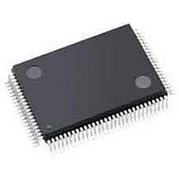
LCMXO640C-3TN100C Lattice, LCMXO640C-3TN100C Datasheet - Page 34

LCMXO640C-3TN100C
Manufacturer Part Number
LCMXO640C-3TN100C
Description
CPLD - Complex Programmable Logic Devices 640 LUTS 74 I/O
Manufacturer
Lattice
Series
MachXOr
Datasheet
1.LCMXO640C-3TN100C.pdf
(95 pages)
Specifications of LCMXO640C-3TN100C
Memory Type
SRAM
Number Of Macrocells
320
Delay Time
4.9 ns
Number Of Programmable I/os
74
Operating Supply Voltage
1.8 V, 2.5 V, 3.3 V
Supply Current
17 mA
Maximum Operating Temperature
+ 90 C
Minimum Operating Temperature
0 C
Package / Case
TQFP-100
Mounting Style
SMD/SMT
Supply Voltage (max)
3.465 V
Supply Voltage (min)
1.71 V
Programmable Type
In System Programmable
Delay Time Tpd(1) Max
4.9ns
Voltage Supply - Internal
1.71 V ~ 3.465 V
Number Of Logic Elements/blocks
-
Number Of Gates
-
Number Of I /o
74
Operating Temperature
0°C ~ 85°C
Mounting Type
*
Lead Free Status / RoHS Status
Lead free / RoHS Compliant
Available stocks
Company
Part Number
Manufacturer
Quantity
Price
Company:
Part Number:
LCMXO640C-3TN100C
Manufacturer:
STC
Quantity:
12 000
Company:
Part Number:
LCMXO640C-3TN100C
Manufacturer:
Lattice Semiconductor Corporation
Quantity:
10 000
Part Number:
LCMXO640C-3TN100C
Manufacturer:
LATTICE
Quantity:
20 000
Lattice Semiconductor
sysIO Differential Electrical Characteristics
LVDS
LVDS Emulation
MachXO devices can support LVDS outputs via emulation (LVDS25E), in addition to the LVDS support that is avail-
able on-chip on certain devices. The output is emulated using complementary LVCMOS outputs in conjunction with
resistors across the driver outputs on all devices. The scheme shown in Figure 3-1 is one possible solution for
LVDS standard implementation. Resistor values in Figure 3-1 are industry standard values for 1% resistors.
Figure 3-1. LVDS Using External Resistors (LVDS25E)
The LVDS differential input buffers are available on certain devices in the MachXO family.
V
V
V
I
V
V
V
ΔV
V
ΔV
I
IN
OSD
Parameter
OH
OL
OD
OS
INP,
THD
CM
Symbol
OD
OS
V
INM
Input Voltage
Differential Input Threshold
Input Common Mode Voltage
Input current
Output high voltage for V
Output low voltage for V
Output voltage differential
Change in V
low
Output voltage offset
Change in V
Output short circuit current
Parameter Description
8mA
8mA
Note: All resistors are ±1%.
OD
OS
VCCIO = 2.5
VCCIO = 2.5
between H and L
between high and
Emulated
On-chip
Buffer
LVDS
Over Recommended Operating Conditions
OP
OP
or V
or V
OM
OM
Off-chip
158
158
100mV ≤ V
200mV ≤ V
350mV ≤ V
Power on
R
R
(V
(V
V
shorted
OD
T
T
OP
OP
= 100 Ohm
= 100 Ohm
= 0V Driver outputs
- V
- V
Test Conditions
140
OM
OM
3-8
THD
THD
THD
), R
)/2, R
T
= 100 Ohm
T
Zo = 100
= 100 Ohm
DC and Switching Characteristics
V
V
V
Off-chip
+/-100
1.125
Min.
0.9V
THD
THD
THD
250
—
—
—
—
—
MachXO Family Data Sheet
0
100
/2
/2
/2
Typ.
1.38
1.03
1.25
350
1.2
1.2
1.2
—
—
—
—
—
—
On-chip
+
-
1.375
+/-10
Max.
1.60
450
2.4
1.8
1.9
2.0
50
50
—
—
6
Units
mV
mV
mV
mV
mA
µA
V
V
V
V
V
V
V


