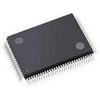
LCMXO640C-3TN100C Lattice, LCMXO640C-3TN100C Datasheet - Page 44

LCMXO640C-3TN100C
Manufacturer Part Number
LCMXO640C-3TN100C
Description
CPLD - Complex Programmable Logic Devices 640 LUTS 74 I/O
Manufacturer
Lattice
Series
MachXOr
Datasheet
1.LCMXO640C-3TN100C.pdf
(95 pages)
Specifications of LCMXO640C-3TN100C
Memory Type
SRAM
Number Of Macrocells
320
Delay Time
4.9 ns
Number Of Programmable I/os
74
Operating Supply Voltage
1.8 V, 2.5 V, 3.3 V
Supply Current
17 mA
Maximum Operating Temperature
+ 90 C
Minimum Operating Temperature
0 C
Package / Case
TQFP-100
Mounting Style
SMD/SMT
Supply Voltage (max)
3.465 V
Supply Voltage (min)
1.71 V
Programmable Type
In System Programmable
Delay Time Tpd(1) Max
4.9ns
Voltage Supply - Internal
1.71 V ~ 3.465 V
Number Of Logic Elements/blocks
-
Number Of Gates
-
Number Of I /o
74
Operating Temperature
0°C ~ 85°C
Mounting Type
*
Lead Free Status / RoHS Status
Lead free / RoHS Compliant
Available stocks
Company
Part Number
Manufacturer
Quantity
Price
Company:
Part Number:
LCMXO640C-3TN100C
Manufacturer:
STC
Quantity:
12 000
Company:
Part Number:
LCMXO640C-3TN100C
Manufacturer:
Lattice Semiconductor Corporation
Quantity:
10 000
Part Number:
LCMXO640C-3TN100C
Manufacturer:
LATTICE
Quantity:
20 000
Lattice Semiconductor
Switching Test Conditions
Figure 3-5 shows the output test load that is used for AC testing. The specific values for resistance, capacitance,
voltage, and other test conditions are shown in Figure 3-5.
Figure 3-5. Output Test Load, LVTTL and LVCMOS Standards
Table 3-5. Test Fixture Required Components, Non-Terminated Interfaces
LVTTL and LVCMOS settings (L -> H, H -> L)
LVTTL and LVCMOS 3.3 (Z -> H)
LVTTL and LVCMOS 3.3 (Z -> L)
Other LVCMOS (Z -> H)
Other LVCMOS (Z -> L)
LVTTL + LVCMOS (H -> Z)
LVTTL + LVCMOS (L -> Z)
Note: Output test conditions for all other interfaces are determined by the respective standards.
Test Condition
DUT
V
R1
T
3-18
188
R
∞
1
CL
0pF
0pF
C
L
Test Poi nt
DC and Switching Characteristics
LVTTL, LVCMOS 3.3 = 1.5V
LVCMOS 2.5 = V
LVCMOS 1.8 = V
LVCMOS 1.5 = V
LVCMOS 1.2 = V
1.5
V
V
V
V
OH
OL
CCIO
CCIO
- 0.15
- 0.15
/2
/2
MachXO Family Data Sheet
Timing Ref.
CCIO
CCIO
CCIO
CCIO
/2
/2
/2
/2
V
V
V
V
V
V
V
—
—
—
—
—
OH
OH
OH
OL
OL
OL
T


