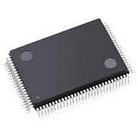
LCMXO256C-3TN100C Lattice, LCMXO256C-3TN100C Datasheet - Page 10

LCMXO256C-3TN100C
Manufacturer Part Number
LCMXO256C-3TN100C
Description
CPLD - Complex Programmable Logic Devices 256 LUTS 78 I/O
Manufacturer
Lattice
Series
MachXOr
Datasheet
1.LCMXO640C-3TN100C.pdf
(95 pages)
Specifications of LCMXO256C-3TN100C
Memory Type
SRAM
Number Of Macrocells
128
Delay Time
4.9 ns
Number Of Programmable I/os
78
Operating Supply Voltage
1.8 V, 2.5 V, 3.3 V
Supply Current
13 mA
Maximum Operating Temperature
+ 90 C
Minimum Operating Temperature
0 C
Package / Case
TQFP-100
Mounting Style
SMD/SMT
Supply Voltage (max)
3.465 V
Supply Voltage (min)
1.71 V
Cpld Type
FLASH
No. Of Macrocells
256
No. Of I/o's
78
Propagation Delay
4.9ns
Global Clock Setup Time
1.8ns
Frequency
420MHz
Supply Voltage Range
1.71V To 3.465V
Rohs Compliant
Yes
Programmable Type
In System Programmable
Delay Time Tpd(1) Max
4.9ns
Voltage Supply - Internal
1.71 V ~ 3.465 V
Number Of Logic Elements/blocks
-
Number Of Gates
-
Number Of I /o
78
Operating Temperature
0°C ~ 85°C
Mounting Type
*
Lead Free Status / RoHS Status
Lead free / RoHS Compliant
Available stocks
Company
Part Number
Manufacturer
Quantity
Price
Company:
Part Number:
LCMXO256C-3TN100C
Manufacturer:
LATTICE
Quantity:
5 600
Company:
Part Number:
LCMXO256C-3TN100C
Manufacturer:
LATTICE
Quantity:
5
Company:
Part Number:
LCMXO256C-3TN100C
Manufacturer:
LATTICE
Quantity:
35
Company:
Part Number:
LCMXO256C-3TN100C
Manufacturer:
Lattice Semiconductor Corporation
Quantity:
10 000
Part Number:
LCMXO256C-3TN100C
Manufacturer:
LATTICE
Quantity:
20 000
Lattice Semiconductor
The ispLEVER design tool takes the output of the synthesis tool and places and routes the design. Generally, the
place and route tool is completely automatic, although an interactive routing editor is available to optimize the
design.
Clock/Control Distribution Network
The MachXO family of devices provides global signals that are available to all PFUs. These signals consist of four
primary clocks and four secondary clocks. Primary clock signals are generated from four 16:1 muxes as shown in
Figure 2-7 and Figure 2-8. The available clock sources for the MachXO256 and MachXO640 devices are four dual
function clock pins and 12 internal routing signals. The available clock sources for the MachXO1200 and
MachXO2280 devices are four dual function clock pins, up to nine internal routing signals and up to six PLL out-
puts.
Figure 2-7. Primary Clocks for MachXO256 and MachXO640 Devices
Routing
12
Clock
Pads
4
2-7
16:1
16:1
16:1
16:1
Primary Clock 0
Primary Clock 1
Primary Clock 2
Primary Clock 3
MachXO Family Data Sheet
Architecture


