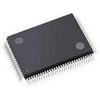
LCMXO256C-3TN100C Lattice, LCMXO256C-3TN100C Datasheet - Page 27

LCMXO256C-3TN100C
Manufacturer Part Number
LCMXO256C-3TN100C
Description
CPLD - Complex Programmable Logic Devices 256 LUTS 78 I/O
Manufacturer
Lattice
Series
MachXOr
Datasheet
1.LCMXO640C-3TN100C.pdf
(95 pages)
Specifications of LCMXO256C-3TN100C
Memory Type
SRAM
Number Of Macrocells
128
Delay Time
4.9 ns
Number Of Programmable I/os
78
Operating Supply Voltage
1.8 V, 2.5 V, 3.3 V
Supply Current
13 mA
Maximum Operating Temperature
+ 90 C
Minimum Operating Temperature
0 C
Package / Case
TQFP-100
Mounting Style
SMD/SMT
Supply Voltage (max)
3.465 V
Supply Voltage (min)
1.71 V
Cpld Type
FLASH
No. Of Macrocells
256
No. Of I/o's
78
Propagation Delay
4.9ns
Global Clock Setup Time
1.8ns
Frequency
420MHz
Supply Voltage Range
1.71V To 3.465V
Rohs Compliant
Yes
Programmable Type
In System Programmable
Delay Time Tpd(1) Max
4.9ns
Voltage Supply - Internal
1.71 V ~ 3.465 V
Number Of Logic Elements/blocks
-
Number Of Gates
-
Number Of I /o
78
Operating Temperature
0°C ~ 85°C
Mounting Type
*
Lead Free Status / RoHS Status
Lead free / RoHS Compliant
Available stocks
Company
Part Number
Manufacturer
Quantity
Price
Company:
Part Number:
LCMXO256C-3TN100C
Manufacturer:
LATTICE
Quantity:
5 600
Company:
Part Number:
LCMXO256C-3TN100C
Manufacturer:
LATTICE
Quantity:
5
Company:
Part Number:
LCMXO256C-3TN100C
Manufacturer:
LATTICE
Quantity:
35
Company:
Part Number:
LCMXO256C-3TN100C
Manufacturer:
Lattice Semiconductor Corporation
Quantity:
10 000
Part Number:
LCMXO256C-3TN100C
Manufacturer:
LATTICE
Quantity:
20 000
www.latticesemi.com
© 2006 Lattice Semiconductor Corp. All Lattice trademarks, registered trademarks, patents, and disclaimers are as listed at www.latticesemi.com/legal. All other brand
or product names are trademarks or registered trademarks of their respective holders. The specifications and information herein are subject to change without notice.
Absolute Maximum Ratings
1. Stress above those listed under the “Absolute Maximum Ratings” may cause permanent damage to the device. Functional operation of the
2. Compliance with the Lattice Thermal Management document is required.
3. All voltages referenced to GND.
4. Overshoot and undershoot of -2V to (V
MachXO256 and MachXO640 Hot Socketing Specifications
1. Insensitive to sequence of V
2. 0 ≤ V
3. I
November 2006
Recommended Operating Conditions
Supply Voltage V
Supply Voltage V
Output Supply Voltage V
I/O Tristate Voltage Applied
Dedicated Input Voltage Applied
Storage Temperature (ambient). . . . . . . . . . . . . . . -65 to 150°C . . . . . . . . . . . . . . . -65 to 150°C
Junction Temp. (Tj) . . . . . . . . . . . . . . . . . . . . . . . . . . +125°C . . . . . . . . . . . . . . . . . . . +125°C
I
V
V
V
t
t
t
t
1. Like power supplies must be tied together. For example, if V
2. See recommended voltages by I/O standard in subsequent table.
3. V
DK
JCOM
JIND
JFLASHCOM
JFLASHIND
CC
CCAUX
CCIO
device at these or any other conditions above those indicated in the operational sections of this specification is not implied.
Symbol
DK
Symbol
and 1.2V V
CC
is additive to I
2
CC
must reach minimum V
3
≤ V
CC
CCIO
Input or I/O leakage Current
Core Supply Voltage for 1.2V Devices
Core Supply Voltage for 1.8V/2.5V/3.3V Devices
Auxiliary Supply Voltage
I/O Driver Supply Voltage
Junction Temperature Commercial Operation
Junction Temperature Industrial Operation
Junction Temperature, Flash Programming, Commercial
Junction Temperature, Flash Programming, Industrial
(MAX), 0 ≤ V
should be tied to V
PU,
CC
CCAUX
I
PD
. . . . . . . . . . . . . . . . . . . . . . . . -0.5 to 1.32V . . . . . . . . . . . . . . . -0.5 to 3.75V
or I
. . . . . . . . . . . . . . . . . . . . . -0.5 to 3.75V . . . . . . . . . . . . . . . -0.5 to 3.75V
CCIO
CCIO
CC,
BH
Parameter
CC
.
V
value before V
4
≤ V
CCAUX,
. . . . . . . . . . . . . . . . . -0.5 to 3.75V . . . . . . . . . . . . . . . -0.5 to 3.75V
. . . . . . . . . . . . . . . . -0.5 to 3.75V . . . . . . . . . . . . . . . -0.5 to 3.75V
CCAUX
CCIO
4
IHMAX
. . . . . . . . . . . . . -0.5 to 3.75V . . . . . . . . . . . . . . . -0.5 to 4.25V
and V
(MAX) and 0 ≤ V
or 1.2V V
+ 2) volts is permitted for a duration of <20ns.
CCAUX
CCIO
1, 2, 3
DC and Switching Characteristics
. However, assumes monotonic rise/fall rates for V
Parameter
CC
reaches 2.5V.
respectively.
0 ≤ V
CCAUX
LCMXO E (1.2V)
CCIO
IN
≤ V
≤ V
and V
3-1
MachXO Family Data Sheet
1
Condition
CCAUX
IH
CC
(MAX)
are both 2.5V, they must also be the same supply. 3.3V V
(MAX).
LCMXO C (1.8V/2.5V/3.3V)
Min.
—
CC,
V
3.135
CCAUX,
Min.
1.14
1.71
1.14
1, 2, 3
Typ.
-40
-40
—
0
0
DC and Switching_01.4
and V
+/-1000
3.465
3.465
3.465
Max.
1.26
CCIO.
+85
100
+85
100
Max
Data Sheet
Units
Units
CCIO
o
o
o
o
µA
V
V
V
V
C
C
C
C


