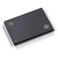
LCMXO256C-3TN100C Lattice, LCMXO256C-3TN100C Datasheet - Page 43

LCMXO256C-3TN100C
Manufacturer Part Number
LCMXO256C-3TN100C
Description
CPLD - Complex Programmable Logic Devices 256 LUTS 78 I/O
Manufacturer
Lattice
Series
MachXOr
Datasheet
1.LCMXO640C-3TN100C.pdf
(95 pages)
Specifications of LCMXO256C-3TN100C
Memory Type
SRAM
Number Of Macrocells
128
Delay Time
4.9 ns
Number Of Programmable I/os
78
Operating Supply Voltage
1.8 V, 2.5 V, 3.3 V
Supply Current
13 mA
Maximum Operating Temperature
+ 90 C
Minimum Operating Temperature
0 C
Package / Case
TQFP-100
Mounting Style
SMD/SMT
Supply Voltage (max)
3.465 V
Supply Voltage (min)
1.71 V
Cpld Type
FLASH
No. Of Macrocells
256
No. Of I/o's
78
Propagation Delay
4.9ns
Global Clock Setup Time
1.8ns
Frequency
420MHz
Supply Voltage Range
1.71V To 3.465V
Rohs Compliant
Yes
Programmable Type
In System Programmable
Delay Time Tpd(1) Max
4.9ns
Voltage Supply - Internal
1.71 V ~ 3.465 V
Number Of Logic Elements/blocks
-
Number Of Gates
-
Number Of I /o
78
Operating Temperature
0°C ~ 85°C
Mounting Type
*
Lead Free Status / RoHS Status
Lead free / RoHS Compliant
Available stocks
Company
Part Number
Manufacturer
Quantity
Price
Company:
Part Number:
LCMXO256C-3TN100C
Manufacturer:
LATTICE
Quantity:
5 600
Company:
Part Number:
LCMXO256C-3TN100C
Manufacturer:
LATTICE
Quantity:
5
Company:
Part Number:
LCMXO256C-3TN100C
Manufacturer:
LATTICE
Quantity:
35
Company:
Part Number:
LCMXO256C-3TN100C
Manufacturer:
Lattice Semiconductor Corporation
Quantity:
10 000
Part Number:
LCMXO256C-3TN100C
Manufacturer:
LATTICE
Quantity:
20 000
Lattice Semiconductor
Flash Download Time
JTAG Port Timing Specifications
t
f
t
t
t
t
t
t
t
t
t
t
t
t
t
t
Rev. A 0.19
REFRESH
MAX
BTCP
BTCPH
BTCPL
BTS
BTH
BTRF
BTCO
BTCODIS
BTCOEN
BTCRS
BTCRH
BUTCO
BTUODIS
BTUPOEN
Symbol
Symbol
Minimum V
(later of the two supplies)
to Device I/O Active
TCK [BSCAN] clock frequency
TCK [BSCAN] clock pulse width
TCK [BSCAN] clock pulse width high
TCK [BSCAN] clock pulse width low
TCK [BSCAN] setup time
TCK [BSCAN] hold time
TCK [BSCAN] rise/fall time
TAP controller falling edge of clock to output valid
TAP controller falling edge of clock to output disabled
TAP controller falling edge of clock to output enabled
BSCAN test capture register setup time
BSCAN test capture register hold time
BSCAN test update register, falling edge of clock to output valid
BSCAN test update register, falling edge of clock to output disabled
BSCAN test update register, falling edge of clock to output enabled
CC
or V
CCAUX
Parameter
LCMXO256
LCMXO640
LCMXO1200
LCMXO2280
Parameter
3-17
Min.
—
—
—
—
DC and Switching Characteristics
MachXO Family Data Sheet
Typ.
—
—
—
—
Min.
40
20
20
10
50
25
—
—
—
—
—
—
—
8
8
Max.
0.4
0.6
0.8
1.0
Max.
25
10
10
10
25
25
25
—
—
—
—
—
—
—
—
Units
mV/ns
ms
ms
ms
ms
Units
MHz
ns
ns
ns
ns
ns
ns
ns
ns
ns
ns
ns
ns
ns


