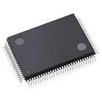
LCMXO256C-3TN100C Lattice, LCMXO256C-3TN100C Datasheet - Page 47

LCMXO256C-3TN100C
Manufacturer Part Number
LCMXO256C-3TN100C
Description
CPLD - Complex Programmable Logic Devices 256 LUTS 78 I/O
Manufacturer
Lattice
Series
MachXOr
Datasheet
1.LCMXO640C-3TN100C.pdf
(95 pages)
Specifications of LCMXO256C-3TN100C
Memory Type
SRAM
Number Of Macrocells
128
Delay Time
4.9 ns
Number Of Programmable I/os
78
Operating Supply Voltage
1.8 V, 2.5 V, 3.3 V
Supply Current
13 mA
Maximum Operating Temperature
+ 90 C
Minimum Operating Temperature
0 C
Package / Case
TQFP-100
Mounting Style
SMD/SMT
Supply Voltage (max)
3.465 V
Supply Voltage (min)
1.71 V
Cpld Type
FLASH
No. Of Macrocells
256
No. Of I/o's
78
Propagation Delay
4.9ns
Global Clock Setup Time
1.8ns
Frequency
420MHz
Supply Voltage Range
1.71V To 3.465V
Rohs Compliant
Yes
Programmable Type
In System Programmable
Delay Time Tpd(1) Max
4.9ns
Voltage Supply - Internal
1.71 V ~ 3.465 V
Number Of Logic Elements/blocks
-
Number Of Gates
-
Number Of I /o
78
Operating Temperature
0°C ~ 85°C
Mounting Type
*
Lead Free Status / RoHS Status
Lead free / RoHS Compliant
Available stocks
Company
Part Number
Manufacturer
Quantity
Price
Company:
Part Number:
LCMXO256C-3TN100C
Manufacturer:
LATTICE
Quantity:
5 600
Company:
Part Number:
LCMXO256C-3TN100C
Manufacturer:
LATTICE
Quantity:
5
Company:
Part Number:
LCMXO256C-3TN100C
Manufacturer:
LATTICE
Quantity:
35
Company:
Part Number:
LCMXO256C-3TN100C
Manufacturer:
Lattice Semiconductor Corporation
Quantity:
10 000
Part Number:
LCMXO256C-3TN100C
Manufacturer:
LATTICE
Quantity:
20 000
Lattice Semiconductor
Power Supply and NC
VCC
VCCIO0
VCCIO1
VCCIO2
VCCIO3
VCCIO4
VCCIO5
VCCIO6
VCCIO7
VCCAUX
GND
NC
1. Pin orientation follows the conventional order from pin 1 marking of the top side view and counter-clockwise.
2. Pin orientation A1 starts from the upper left corner of the top side view with alphabetical order ascending vertically and numerical order ascending horizontally.
3. All grounds must be electrically connected at the board level. For fpBGA and ftBGA packages, the total number of GND balls is less than the actual number of
4. NC pins should not be connected to any active signals, VCC or GND.
GND logic connections from the die to the common package GND plane.
4
Signal
3
LCMXO256/640: 35, 90
LCMXO1200/2280: 17, 35, 66, 91
LCMXO256: 60, 74, 92
LCMXO640: 80, 92
LCMXO1200/2280: 94
LCMXO256: 10, 24, 41
LCMXO640: 60, 74
LCMXO1200/2280: 80
LCMXO256: None
LCMXO640: 29, 41
LCMXO1200/2280: 70
LCMXO256: None
LCMXO640: 10, 24
LCMXO1200/2280: 56
LCMXO256/640: None
LCMXO1200/2280: 44
LCMXO256/640: None
LCMXO1200/2280: 27
LCMXO256/640: None
LCMXO1200/2280: 20
LCMXO256/640: None
LCMXO1200/2280: 6
LCMXO256/640: 88
LCMXO1200/2280: 36, 90
LCMXO256: 40, 84, 62, 75, 93, 12,
25, 42
LCMXO640: 40, 84, 81, 93, 62, 75,
30, 42, 12, 25
LCMXO1200/2280: 9, 41, 59, 83,
100, 76, 50, 26
100 TQFP
1
21, 52, 93, 129
LCMXO640: 117, 135
LCMXO1200/2280: 135
LCMXO640: 82, 98
LCMXO1200/2280: 117
LCMXO640: 38, 63
LCMXO1200/2280: 98
LCMXO640: 10, 26
LCMXO1200/2280: 82
LCMXO640: None
LCMXO1200/2280: 63
LCMXO640: None
LCMXO1200/2280: 38
LCMXO640: None
LCMXO1200/2280: 26
LCMXO640: None
LCMXO1200/2280: 10
53, 128
16, 59, 88, 123, 118, 136, 83, 99,
37, 64, 11, 27
4-3
144 TQFP
1
MachXO Family Data Sheet
LCMXO256: H14, A14, B5
LCMXO640: B12, B5
LCMXO256: G1, P1, P10
LCMXO640: H14, A14
LCMXO256: None
LCMXO640: P4, P10
LCMXO256: None
LCMXO640: G1, P1
—
—
—
—
LCMXO256: N9, B9, G14, B13,
A4, H1, N2, N10
LCMXO640: N9, B9, A10, A4,
G14, B13, N3, N10, H1, N2
—
P7, B6
B7
Pinout Information
100 csBGA
2


