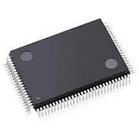
LCMXO256C-3TN100C Lattice, LCMXO256C-3TN100C Datasheet - Page 7

LCMXO256C-3TN100C
Manufacturer Part Number
LCMXO256C-3TN100C
Description
CPLD - Complex Programmable Logic Devices 256 LUTS 78 I/O
Manufacturer
Lattice
Series
MachXOr
Datasheet
1.LCMXO640C-3TN100C.pdf
(95 pages)
Specifications of LCMXO256C-3TN100C
Memory Type
SRAM
Number Of Macrocells
128
Delay Time
4.9 ns
Number Of Programmable I/os
78
Operating Supply Voltage
1.8 V, 2.5 V, 3.3 V
Supply Current
13 mA
Maximum Operating Temperature
+ 90 C
Minimum Operating Temperature
0 C
Package / Case
TQFP-100
Mounting Style
SMD/SMT
Supply Voltage (max)
3.465 V
Supply Voltage (min)
1.71 V
Cpld Type
FLASH
No. Of Macrocells
256
No. Of I/o's
78
Propagation Delay
4.9ns
Global Clock Setup Time
1.8ns
Frequency
420MHz
Supply Voltage Range
1.71V To 3.465V
Rohs Compliant
Yes
Programmable Type
In System Programmable
Delay Time Tpd(1) Max
4.9ns
Voltage Supply - Internal
1.71 V ~ 3.465 V
Number Of Logic Elements/blocks
-
Number Of Gates
-
Number Of I /o
78
Operating Temperature
0°C ~ 85°C
Mounting Type
*
Lead Free Status / RoHS Status
Lead free / RoHS Compliant
Available stocks
Company
Part Number
Manufacturer
Quantity
Price
Company:
Part Number:
LCMXO256C-3TN100C
Manufacturer:
LATTICE
Quantity:
5 600
Company:
Part Number:
LCMXO256C-3TN100C
Manufacturer:
LATTICE
Quantity:
5
Company:
Part Number:
LCMXO256C-3TN100C
Manufacturer:
LATTICE
Quantity:
35
Company:
Part Number:
LCMXO256C-3TN100C
Manufacturer:
Lattice Semiconductor Corporation
Quantity:
10 000
Part Number:
LCMXO256C-3TN100C
Manufacturer:
LATTICE
Quantity:
20 000
Lattice Semiconductor
There are 14 input signals: 13 signals from routing and one from the carry-chain (from the adjacent Slice/PFU).
There are 7 outputs: 6 to the routing and one to the carry-chain (to the adjacent Slice/PFU). Table 2-1 lists the sig-
nals associated with each Slice.
Figure 2-5. Slice Diagram
Table 2-1. Slice Signal Descriptions
1. See Figure 2-4 for connection details.
2. Requires two PFUs.
Function
Control Signals
selected and
inverted per
Slice in routing
Notes:
Some inter-Slice signals are not shown.
* Only PFUs at the edges have fast connections to the I/O cell.
Output
Output
Output
Output
Output
Input
Input
Input
Input
Input
Input
Input
From
Routing
Inter-PFU signal
Inter-PFU signal
Control signal
Control signal
Control signal
Multi-purpose
Data signals
Data signals
Data signals
Data signals
Data signal
Data signal
CLK
LSR
Type
M1
M0
CE
C1
D1
C0
D0
A1
B1
A0
B0
A0, B0, C0, D0 Inputs to LUT4
A1, B1, C1, D1 Inputs to LUT4
Signal Names
To Adjacent Slice/PFU
From Adjacent Slice/PFU
Q0, Q1
M0/M1
F0, F1
OFX0
OFX1
FCIN
FCO
LSR
CLK
CE
LUT4 &
CARRY
LUT4 &
CARRY
CO
CO
CI
CI
SUM
SUM
F
F
Multipurpose Input
Clock Enable
Local Set/Reset
System Clock
Fast Carry In
LUT4 output register bypass signals
Register Outputs
Output of a LUT5 MUX
Output of a LUT6, LUT7, LUT8
Fast Carry Out
2-4
OFX0
Expansion
LUT
Mux
1
1
Slice
D
D
Description
Latch
Latch
FF/
FF/
MachXO Family Data Sheet
2
MUX depending on the Slice
OFX1
F1
OFX0
F0
Q0
Fast Connection
to I/O Cell*
Q1
Fast Connection
to I/O Cell*
Architecture
To
Routing


