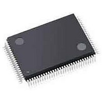
A3PN030-ZVQG100 Actel, A3PN030-ZVQG100 Datasheet - Page 11

A3PN030-ZVQG100
Manufacturer Part Number
A3PN030-ZVQG100
Description
FPGA - Field Programmable Gate Array 30K System Gates ProASIC3 nano
Manufacturer
Actel
Datasheet
1.A3PN030-ZVQG100.pdf
(106 pages)
Specifications of A3PN030-ZVQG100
Processor Series
A3PN030
Core
IP Core
Number Of Macrocells
256
Maximum Operating Frequency
350 MHz
Number Of Programmable I/os
77
Supply Voltage (max)
3.3 V
Supply Current
2 mA
Maximum Operating Temperature
+ 70 C
Minimum Operating Temperature
- 20 C
Development Tools By Supplier
AGLN-Nano-Kit, AGLN-Z-Nano-Kit, Silicon-Explorer II, Silicon-Sculptor 3, SI-EX-TCA, FloasPro 4, FlashPro 3, FlashPro Lite
Mounting Style
SMD/SMT
Supply Voltage (min)
1.5 V
Number Of Gates
30 K
Package / Case
VQFP-100
Lead Free Status / RoHS Status
Lead free / RoHS Compliant
Available stocks
Company
Part Number
Manufacturer
Quantity
Price
Company:
Part Number:
A3PN030-ZVQG100
Manufacturer:
ACTEL
Quantity:
1 213
Company:
Part Number:
A3PN030-ZVQG100
Manufacturer:
Microsemi SoC
Quantity:
10 000
Company:
Part Number:
A3PN030-ZVQG100I
Manufacturer:
NXP
Quantity:
4 600
Company:
Part Number:
A3PN030-ZVQG100I
Manufacturer:
Microsemi SoC
Quantity:
10 000
Figure 1-5 • VersaTile Configurations
X1
X2
X3
LUT-3 Equivalent
LUT-3
In addition, extensive on-chip programming circuitry allows for rapid, single-voltage (3.3 V) programming
of ProASIC3 nano devices via an IEEE 1532 JTAG interface.
VersaTiles
The ProASIC3 nano core consists of VersaTiles, which have been enhanced beyond the ProASIC
core tiles. The ProASIC3 nano VersaTile supports the following:
Refer to
User Nonvolatile FlashROM
Actel ProASIC3 nano devices have 1 kbit of on-chip, user-accessible, nonvolatile FlashROM. The
FlashROM can be used in diverse system applications:
The FlashROM is written using the standard ProASIC3 nano IEEE 1532 JTAG programming interface.
The core can be individually programmed (erased and written), and on-chip AES decryption can be used
selectively to securely load data over public networks (except in the A3PN030 and smaller devices), as in
security keys stored in the FlashROM for a user design.
The FlashROM can be programmed via the JTAG programming interface, and its contents can be read
back either through the JTAG programming interface or via direct FPGA core addressing. Note that the
FlashROM can only be programmed from the JTAG interface and cannot be programmed from the
internal logic array.
The FlashROM is programmed as 8 banks of 128 bits; however, reading is performed on a byte-by-byte
basis using a synchronous interface. A 7-bit address from the FPGA core defines which of the 8 banks
and which of the 16 bytes within that bank are being read. The three most significant bits (MSBs) of the
FlashROM address determine the bank, and the four least significant bits (LSBs) of the FlashROM
address define the byte.
The Actel ProASIC3 nano development software solutions, Libero
and Designer, have extensive support for the FlashROM. One such feature is auto-generation of
sequential programming files for applications requiring a unique serial number in each part. Another
feature enables the inclusion of static data for system version control. Data for the FlashROM can be
generated quickly and easily using Actel Libero IDE and Designer software tools. Comprehensive
•
•
•
•
•
•
•
•
•
•
•
•
All 3-input logic functions—LUT-3 equivalent
Latch with clear or set
D-flip-flop with clear or set
Enable D-flip-flop with clear or set
Internet protocol addressing (wireless or fixed)
System calibration settings
Device serialization and/or inventory control
Subscription-based business models (for example, set-top boxes)
Secure key storage for secure communications algorithms
Asset management/tracking
Date stamping
Version management
Y
Figure 1-5
for VersaTile configurations.
D-Flip-Flop with Clear or Set
Data
CLK
CLR
D-FF
R e v i s i o n 8
Y
Enable D-Flip-Flop with Clear or Set
Enable
®
Data
CLK
Integrated Design Environment (IDE)
CLR
ProASIC3 nano Flash FPGAs
D-FF
Y
PLUS®
1 -5


