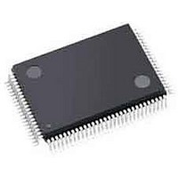
A3PN250-ZVQG100 Actel, A3PN250-ZVQG100 Datasheet - Page 10

A3PN250-ZVQG100
Manufacturer Part Number
A3PN250-ZVQG100
Description
FPGA - Field Programmable Gate Array 250K System Gates ProASIC3 nano
Manufacturer
Actel
Datasheet
1.A3PN030-ZVQG100.pdf
(106 pages)
Specifications of A3PN250-ZVQG100
Processor Series
A3PN250
Core
IP Core
Number Of Macrocells
2048
Maximum Operating Frequency
350 MHz
Number Of Programmable I/os
68
Data Ram Size
36 Kbit
Delay Time
1.05 ns
Supply Voltage (max)
3.3 V
Supply Current
3 mA
Maximum Operating Temperature
+ 70 C
Minimum Operating Temperature
- 20 C
Development Tools By Supplier
AGLN-Nano-Kit, AGLN-Z-Nano-Kit, Silicon-Explorer II, Silicon-Sculptor 3, SI-EX-TCA, FloasPro 4, FlashPro 3, FlashPro Lite
Mounting Style
SMD/SMT
Supply Voltage (min)
1.5 V
Number Of Gates
250 K
Package / Case
VQFP-100
Lead Free Status / RoHS Status
Lead free / RoHS Compliant
Available stocks
Company
Part Number
Manufacturer
Quantity
Price
Company:
Part Number:
A3PN250-ZVQG100
Manufacturer:
ACT
Quantity:
19
Company:
Part Number:
A3PN250-ZVQG100
Manufacturer:
Microsemi SoC
Quantity:
10 000
Company:
Part Number:
A3PN250-ZVQG100I
Manufacturer:
Microsemi SoC
Quantity:
10 000
ProASIC3 nano Device Overview
Figure 1-3 • ProASIC3 nano Device Architecture Overview with Two I/O Banks (A3PN060 and A3PN125)
Figure 1-4 • ProASIC3 nano Device Architecture Overview with Four I/O Banks (A3PN250)
1 - 4
The FPGA core consists of a sea of VersaTiles. Each VersaTile can be configured as a three-input logic
function, a D-flip-flop (with or without enable), or a latch by programming the appropriate flash switch
interconnections. The versatility of the ProASIC3 nano core tile as either a three-input lookup table (LUT)
equivalent or as a D-flip-flop/latch with enable allows for efficient use of the FPGA fabric. The VersaTile
capability is unique to the Actel ProASIC3 family of third-generation architecture flash FPGAs. VersaTiles
are connected with any of the four levels of routing hierarchy. Flash switches are distributed throughout
the device to provide nonvolatile, reconfigurable interconnect programming. Maximum core utilization is
possible for virtually any design.
Decryption
Decryption
ISP AES
ISP AES
User Nonvolatile
User Nonvolatile
FlashROM
FlashROM
Bank 0
Bank 1
Bank 0
Bank 2
R e vi s i o n 8
Charge Pumps
Charge Pumps
CCC
RAM Block
4,608-Bit Dual-Port
SRAM or FIFO Block
I/Os
VersaTile
CCC
RAM Block
4,608-Bit Dual-Port
SRAM or FIFO Block
I/Os
VersaTile


