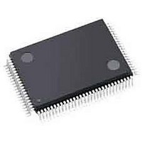
A3PN060-ZVQG100 Actel, A3PN060-ZVQG100 Datasheet - Page 103

A3PN060-ZVQG100
Manufacturer Part Number
A3PN060-ZVQG100
Description
FPGA - Field Programmable Gate Array 60K System Gates ProASIC3 nano
Manufacturer
Actel
Datasheet
1.A3PN030-ZVQG100.pdf
(106 pages)
Specifications of A3PN060-ZVQG100
Processor Series
A3PN060
Core
IP Core
Number Of Macrocells
512
Maximum Operating Frequency
350 MHz
Number Of Programmable I/os
71
Data Ram Size
18 Kbit
Delay Time
0.96 ns
Supply Voltage (max)
3.3 V
Supply Current
2 mA
Maximum Operating Temperature
+ 70 C
Minimum Operating Temperature
- 20 C
Development Tools By Supplier
AGLN-Nano-Kit, AGLN-Z-Nano-Kit, Silicon-Explorer II, Silicon-Sculptor 3, SI-EX-TCA, FloasPro 4, FlashPro 3, FlashPro Lite
Mounting Style
SMD/SMT
Supply Voltage (min)
1.5 V
Number Of Gates
60 K
Package / Case
VQFP-100
Lead Free Status / RoHS Status
Lead free / RoHS Compliant
Available stocks
Company
Part Number
Manufacturer
Quantity
Price
Company:
Part Number:
A3PN060-ZVQG100
Manufacturer:
Microsemi SoC
Quantity:
10 000
Company:
Part Number:
A3PN060-ZVQG100I
Manufacturer:
Microsemi SoC
Quantity:
10 000
Revision
Revision 1 (cont’d)
DC and Switching
Characteristics
Advance v0.2
Packaging Advance
v0.2
The
table note 4: "For nano devices, the VQ100 package is offered in both leaded and
RoHS-compliant versions. All other packages are RoHS-compliant only."
The
updated to remove QN100 for A3PN250.
The
number of gates and dual-port RAM for ProASIC3 nano devices.
The device architecture figures,
Overview with Two I/O Banks (A3PN060 and A3PN125)
ProASIC3 nano Device Architecture Overview with Four I/O Banks
were revised.
Banks and No RAM (A3PN010 and A3PN030)
The
A3PN020 and smaller devices.
Table 2-2 • Recommended Operating Conditions
the VCCI row. The following table note was added: "VMV pins must be connected
to the corresponding VCCI pins."
The values in
for A3PN010, A3PN015, and A3PN020.
A table note, "All LVCMOS 3.3 V software macros support LVCMOS 3.3 V wide
range, as specified in the JESD8-B specification," was added to
Summary of Maximum and Minimum DC Input and Output
Summary of I/O Timing Characteristics—Software Default Settings (at 35
and
Settings (at 10
3.3 V LVCMOS Wide Range was added to
Maximum Resistances
The
Note 2 for the
was added/changed to "The die attach paddle of the package is tied to ground
(GND)."
The
left corner instead of the upper right corner.
"PLL and CCC" section
"48-Pin QFN"
"General Description" section
"100-Pin VQFP"
"I/Os Per Package"
"ProASIC3 nano Product Available in the Z Feature Grade" section
Table 2-19 • Summary of I/O Timing Characteristics—Software Default
Figure 1-1 • ProASIC3 Device Architecture Overview with Two I/O
Table 2-7 • Quiescent Supply Current Characteristics
pF).
"48-Pin
pin diagram was revised.
pin diagram was revised to move the pin IDs to the upper
1
QFN",
and
table was updated to add the following information to
was revised to include information about CCC-GLs in
Table 2-23 • I/O Short Currents I
"68-Pin
Figure 1-3 • ProASIC3 nano Device Architecture
R e v i s i o n 8
was updated to give correct information about
Changes
QFN", and
is new.
Table 2-21 • I/O Output Buffer
1, 2
"100-Pin VQFP"
was revised to add VMV to
through
Levels,
OSH
/I
OSL
ProASIC3 nano Flash FPGAs
pin diagrams
were revised
Figure 1-4 •
Table 2-14 •
Table 2-18 •
(A3PN250),
.
was
pF),
2-16,
2-19,
3-2, 3-5,
through
Page
1-1
1-3
1-4
1-6
2-2
2-6
3-2
3-9
3-9
IV
II
2-18
2-20
4 -3


