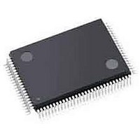
A3PN060-ZVQG100 Actel, A3PN060-ZVQG100 Datasheet - Page 50

A3PN060-ZVQG100
Manufacturer Part Number
A3PN060-ZVQG100
Description
FPGA - Field Programmable Gate Array 60K System Gates ProASIC3 nano
Manufacturer
Actel
Datasheet
1.A3PN030-ZVQG100.pdf
(106 pages)
Specifications of A3PN060-ZVQG100
Processor Series
A3PN060
Core
IP Core
Number Of Macrocells
512
Maximum Operating Frequency
350 MHz
Number Of Programmable I/os
71
Data Ram Size
18 Kbit
Delay Time
0.96 ns
Supply Voltage (max)
3.3 V
Supply Current
2 mA
Maximum Operating Temperature
+ 70 C
Minimum Operating Temperature
- 20 C
Development Tools By Supplier
AGLN-Nano-Kit, AGLN-Z-Nano-Kit, Silicon-Explorer II, Silicon-Sculptor 3, SI-EX-TCA, FloasPro 4, FlashPro 3, FlashPro Lite
Mounting Style
SMD/SMT
Supply Voltage (min)
1.5 V
Number Of Gates
60 K
Package / Case
VQFP-100
Lead Free Status / RoHS Status
Lead free / RoHS Compliant
Available stocks
Company
Part Number
Manufacturer
Quantity
Price
Company:
Part Number:
A3PN060-ZVQG100
Manufacturer:
Microsemi SoC
Quantity:
10 000
Company:
Part Number:
A3PN060-ZVQG100I
Manufacturer:
Microsemi SoC
Quantity:
10 000
ProASIC3 nano DC and Switching Characteristics
Table 2-50 • Minimum and Maximum DC Input and Output Levels
Figure 2-9 • AC Loading
Table 2-51 • 1.5 V LVCMOS AC Waveforms, Measuring Points, and Capacitive Loads
2- 36
1.5 V LVCMOS
Drive Strength
2 mA
Notes:
1. I
2. I
3. Currents are measured at high temperature (100°C junction temperature) and maximum voltage.
4. Currents are measured at 85°C junction temperature.
5. Software default selection highlighted in gray.
Input LOW (V)
0
Notes:
1. Measuring point = Vtrip. See
2. Capacitive Load for A3PN060, A3PN125, and A3PN250 is 35 pF.
larger when operating outside recommended ranges.
IL
IH
is the input leakage current per I/O pin over recommended operation conditions where –0.3 V < VIN < VIL.
is the input leakage current per I/O pin over recommended operating conditions VIH < VIN < VCCI. Input current is
1.5 V LVCMOS (JESD8-11)
Low-Voltage CMOS for 1.5 V is an extension of the LVCMOS standard (JESD8-5) used for general-
purpose 1.5 V applications. It uses a 1.5 V input buffer and a push-pull output buffer.
Min.
–0.3 0.35 * VCCI
Test Point
Datapath
V
VIL
Max.
V
Table 2-16 on page 2-17
35 pF
Input HIGH (V)
0.65 *
VCCI
Min.
V
1.5
VIH
Enable Path
Test Point
Max.
3.6
V
R = 1 k
for a complete table of trip points.
0.25 * VCCI 0.75 * VCCI
R e visio n 8
Max.
VOL
V
Measuring Point* (V)
R to VCCI for t
R to GND for t
35 pF for t
5 pF for t
0.75
VOH
Min.
V
HZ
ZH
/ t
/ t
mA mA
LZ
I
HZ
LZ
OL
2
ZHS
/ t
/ t
I
OH
ZL
ZH
2
/ t
ZL
/ t
/ t
Max.
mA
ZLS
I
ZHS
/ t
OSL
13
ZLS
3
C
LOAD
Max.
I
mA
10
OSH
16
(pF)
3
µA
I
IL
10
1
4
I
µA
IH
10
2
4


