A3PN060-ZVQG100 Actel, A3PN060-ZVQG100 Datasheet - Page 8
A3PN060-ZVQG100
Manufacturer Part Number
A3PN060-ZVQG100
Description
FPGA - Field Programmable Gate Array 60K System Gates ProASIC3 nano
Manufacturer
Actel
Datasheet
1.A3PN030-ZVQG100.pdf
(106 pages)
Specifications of A3PN060-ZVQG100
Processor Series
A3PN060
Core
IP Core
Number Of Macrocells
512
Maximum Operating Frequency
350 MHz
Number Of Programmable I/os
71
Data Ram Size
18 Kbit
Delay Time
0.96 ns
Supply Voltage (max)
3.3 V
Supply Current
2 mA
Maximum Operating Temperature
+ 70 C
Minimum Operating Temperature
- 20 C
Development Tools By Supplier
AGLN-Nano-Kit, AGLN-Z-Nano-Kit, Silicon-Explorer II, Silicon-Sculptor 3, SI-EX-TCA, FloasPro 4, FlashPro 3, FlashPro Lite
Mounting Style
SMD/SMT
Supply Voltage (min)
1.5 V
Number Of Gates
60 K
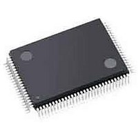
Package / Case
VQFP-100
Lead Free Status / RoHS Status
Lead free / RoHS Compliant
Available stocks
Company
Part Number
Manufacturer
Quantity
Price
Company:

Part Number:
A3PN060-ZVQG100
Manufacturer:
Microsemi SoC
Quantity:
10 000
Company:
Part Number:
A3PN060-ZVQG100I
Manufacturer:
Microsemi SoC
Quantity:
10 000


ProASIC3 nano Device Overview
1 - 2
to make invasive attacks extremely difficult. ProASIC3 nano devices, with FlashLock and AES security,
are unique in being highly resistant to both invasive and noninvasive attacks. Your valuable IP is
protected and secure, making remote ISP possible. A ProASIC3 nano device provides the most
impenetrable security for programmable logic designs.
Single Chip
Flash-based FPGAs store their configuration information in on-chip flash cells. Once programmed, the
configuration data is an inherent part of the FPGA structure, and no external configuration data needs to
be loaded at system power-up (unlike SRAM-based FPGAs). Therefore, flash-based ProASIC3 nano
FPGAs do not require system configuration components such as EEPROMs or microcontrollers to load
device configuration data. This reduces bill-of-materials costs and PCB area, and increases security and
system reliability.
Live at Power-Up
Actel flash-based ProASIC3 nano devices support Level 0 of the LAPU classification standard. This
feature helps in system component initialization, execution of critical tasks before the processor wakes
up, setup and configuration of memory blocks, clock generation, and bus activity management. The
LAPU feature of flash-based ProASIC3 nano devices greatly simplifies total system design and reduces
total system cost, often eliminating the need for CPLDs and clock generation PLLs that are used for
these purposes in a system. In addition, glitches and brownouts in system power will not corrupt the
ProASIC3 nano device's flash configuration, and unlike SRAM-based FPGAs, the device will not have to
be reloaded when system power is restored. This enables the reduction or complete removal of the
configuration PROM, expensive voltage monitor, brownout detection, and clock generator devices from
the PCB design. Flash-based ProASIC3 nano devices simplify total system design and reduce cost and
design risk while increasing system reliability and improving system initialization time.
Firm Errors
Firm errors occur most commonly when high-energy neutrons, generated in the upper atmosphere, strike
a configuration cell of an SRAM FPGA. The energy of the collision can change the state of the
configuration cell and thus change the logic, routing, or I/O behavior in an unpredictable way. These
errors are impossible to prevent in SRAM FPGAs. The consequence of this type of error can be a
complete system failure. Firm errors do not exist in the configuration memory of ProASIC3 nano flash-
based FPGAs. Once it is programmed, the flash cell configuration element of ProASIC3 nano FPGAs
cannot be altered by high-energy neutrons and is therefore immune to them. Recoverable (or soft) errors
occur in the user data SRAM of all FPGA devices. These can easily be mitigated by using error detection
and correction (EDAC) circuitry built into the FPGA fabric.
Low Power
Flash-based ProASIC3 nano devices exhibit power characteristics similar to an ASIC, making them an
ideal choice for power-sensitive applications. ProASIC3 nano devices have only a very limited power-on
current surge and no high-current transition period, both of which occur on many FPGAs.
ProASIC3 nano devices also have low dynamic power consumption to further maximize power savings.
Advanced Flash Technology
ProASIC3 nano devices offer many benefits, including nonvolatility and reprogrammability through an
advanced flash-based, 130-nm LVCMOS process with seven layers of metal. Standard CMOS design
techniques are used to implement logic and control functions. The combination of fine granularity,
enhanced flexible routing resources, and abundant flash switches allows for very high logic utilization
without compromising device routability or performance. Logic functions within the device are
interconnected through a four-level routing hierarchy.
Advanced Architecture
The proprietary ProASIC3 nano architecture provides granularity comparable to standard-cell ASICs.
The ProASIC3 nano device consists of five distinct and programmable architectural features
to
Figure 1-4 on page
•
FPGA VersaTiles
1-4):
R e vi s i o n 8
(Figure 1-3
Related parts for A3PN060-ZVQG100
Image
Part Number
Description
Manufacturer
Datasheet
Request
R

Part Number:
Description:
A3PN060-VQG100I
Manufacturer:
Actel
Datasheet:
Part Number:
Description:
Manufacturer:
Actel
Datasheet:
Part Number:
Description:
TQFP 100/IC,FPGA,1536-CELL,CMOS
Manufacturer:
Actel
Datasheet:
Part Number:
Description:
Manufacturer:
Actel
Datasheet:

Part Number:
Description:
Proasic 3 Nano Flash Fpgas
Manufacturer:
Actel Corporation
Datasheet:
Part Number:
Description:
MCU, MPU & DSP Development Tools Silicon Sculptor Programming Mod
Manufacturer:
Actel
Part Number:
Description:
MCU, MPU & DSP Development Tools InSystem Programming ProASICPLUS Devices
Manufacturer:
Actel
Part Number:
Description:
Programming Socket Adapters & Emulators PQ160 Module
Manufacturer:
Actel
Part Number:
Description:
Programming Socket Adapters & Emulators Axcelerator Adap Module Kit
Manufacturer:
Actel
Part Number:
Description:
Programming Socket Adapters & Emulators Evaluation
Manufacturer:
Actel
Part Number:
Description:
Programming Socket Adapters & Emulators AFDX Solutions
Manufacturer:
Actel
Part Number:
Description:
Programming Socket Adapters & Emulators SILICON SCULPTOR ADAPTER MODULE
Manufacturer:
Actel
Datasheet:
Part Number:
Description:
Programming Socket Adapters & Emulators Axcelerator Adap Module Kit
Manufacturer:
Actel
Part Number:
Description:
Programming Socket Adapters & Emulators Evaluation
Manufacturer:
Actel
Part Number:
Description:
Programming Socket Adapters & Emulators Silicon Sculptor Software
Manufacturer:
Actel