A3PN030-ZQNG68 Actel, A3PN030-ZQNG68 Datasheet - Page 101
A3PN030-ZQNG68
Manufacturer Part Number
A3PN030-ZQNG68
Description
FPGA - Field Programmable Gate Array 30K System Gates ProASIC3 nano
Manufacturer
Actel
Datasheet
1.A3PN030-ZVQG100.pdf
(106 pages)
Specifications of A3PN030-ZQNG68
Processor Series
A3PN030
Core
IP Core
Number Of Macrocells
256
Maximum Operating Frequency
350 MHz
Number Of Programmable I/os
49
Supply Voltage (max)
3.3 V
Supply Current
2 mA
Maximum Operating Temperature
+ 70 C
Minimum Operating Temperature
- 20 C
Development Tools By Supplier
AGLN-Nano-Kit, AGLN-Z-Nano-Kit, Silicon-Explorer II, Silicon-Sculptor 3, SI-EX-TCA, FloasPro 4, FlashPro 3, FlashPro Lite
Mounting Style
SMD/SMT
Supply Voltage (min)
1.5 V
Number Of Gates
30 K
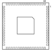
Package / Case
QFN-68
Lead Free Status / RoHS Status
Lead free / RoHS Compliant
Available stocks
Company
Part Number
Manufacturer
Quantity
Price
Company:

Part Number:
A3PN030-ZQNG68I
Manufacturer:
ACT
Quantity:
5


4 – Datasheet Information
List of Changes
Revision
July 2010
Revision 8 (Apr 2010) References to differential inputs were removed from the datasheet, since
The following table lists critical changes that were made in each revision of the ProASIC3 nano
datasheet.
The versioning system for datasheets has been changed. Datasheets are
assigned a revision number that increments each time the datasheet is revised.
The
device in the device family.
ProASIC3 nano devices do not support differential inputs (SAR 21449).
The
The JTAG DC voltage was revised in
Conditions
voltage (operation mode) was changed from 3.45 V to 3.6 V (SAR 25220).
The highest temperature in
for Timing Delays
The typical value for A3PN010 was revised in
Current
values do not include I/O static contribution.
The following tables were updated with available information:
Table 2-8 • Summary of I/O Input Buffer Power (Per Pin) – Default I/O Software
Settings
Table 2-9 • Summary of I/O Output Buffer Power (per pin) – Default I/O Software
Settings
Table 2-10 • Different Components Contributing to Dynamic Power Consumption
in ProASIC3 nano Devices
Table 2-14 • Summary of Maximum and Minimum DC Input and Output Levels
Table 2-18 • Summary of I/O Timing Characteristics—Software Default Settings
(at 35 pF)
Table 2-19 • Summary of I/O Timing Characteristics—Software Default Settings
(at 10 pF)
Table 2-22 • I/O Weak Pull-Up/Pull-Down Resistances
range data and correct the formulas in the table notes (SAR 21348).
The text introducing
was revised to state six months at 100° instead of three months at 110° for
reliability concerns. The row for 110° was removed from the table.
Table 2-26 • I/O Input Rise Time, Fall Time, and Related I/O Reliability
revised to give values with Schmitt trigger disabled and enabled (SAR 24634).
The temperature for reliability was changed to 100ºC.
Table 2-33 • Minimum and Maximum DC Input and Output Levels for 3.3 V
LVCMOS Wide Range
Characteristics" section
tables for 3.3 V LVCMOS wide range are new.
"ProASIC3 nano Device Status" table on page II
"ProASIC3 nano Device Status" table
1
Characteristics. The note was revised to remove the statement that
1, 2
(SAR 24052). The maximum value for VPUMP programming
was changed to 100ºC.
Table 2-24 • Duration of Short Circuit Event before Failure
were updated with available information. The timing
and the timing tables in the
Table 2-6 • Temperature and Voltage Derating Factors
R e v i s i o n 8
Changes
Table 2-2 • Recommended Operating
is new.
Table 2-7 • Quiescent Supply
indicates the status for each
was revised to add wide
"Single-Ended I/O
was
through
Page
2-18
2-19
2-20
2-21
2-22
N/A
N/A
2-2
2-5
2-6
2-6
II
4 -1
Related parts for A3PN030-ZQNG68
Image
Part Number
Description
Manufacturer
Datasheet
Request
R

Part Number:
Description:
FPGA - Field Programmable Gate Array 30K System Gates ProASIC3 nano
Manufacturer:
Actel
Datasheet:

Part Number:
Description:
FPGA - Field Programmable Gate Array 30K System Gates ProASIC3 nano
Manufacturer:
Actel
Datasheet:

Part Number:
Description:
A3PN030-ZVQG100I
Manufacturer:
Actel
Datasheet:
Part Number:
Description:
Manufacturer:
Actel
Datasheet:
Part Number:
Description:
Manufacturer:
Actel
Datasheet:
Part Number:
Description:
Manufacturer:
Actel
Datasheet:
Part Number:
Description:
Manufacturer:
Actel
Datasheet:
Part Number:
Description:
Manufacturer:
Actel
Datasheet:
Part Number:
Description:
MCU, MPU & DSP Development Tools Silicon Sculptor Programming Mod
Manufacturer:
Actel
Part Number:
Description:
MCU, MPU & DSP Development Tools InSystem Programming ProASICPLUS Devices
Manufacturer:
Actel
Part Number:
Description:
Programming Socket Adapters & Emulators PQ160 Module
Manufacturer:
Actel
Part Number:
Description:
Programming Socket Adapters & Emulators Axcelerator Adap Module Kit
Manufacturer:
Actel
Part Number:
Description:
Programming Socket Adapters & Emulators Evaluation
Manufacturer:
Actel
Part Number:
Description:
Programming Socket Adapters & Emulators AFDX Solutions
Manufacturer:
Actel
Part Number:
Description:
Programming Socket Adapters & Emulators SILICON SCULPTOR ADAPTER MODULE
Manufacturer:
Actel
Datasheet: