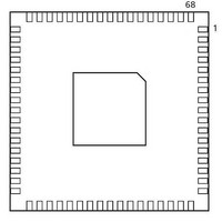
A3PN030-ZQNG68 Actel, A3PN030-ZQNG68 Datasheet - Page 57

A3PN030-ZQNG68
Manufacturer Part Number
A3PN030-ZQNG68
Description
FPGA - Field Programmable Gate Array 30K System Gates ProASIC3 nano
Manufacturer
Actel
Datasheet
1.A3PN030-ZVQG100.pdf
(106 pages)
Specifications of A3PN030-ZQNG68
Processor Series
A3PN030
Core
IP Core
Number Of Macrocells
256
Maximum Operating Frequency
350 MHz
Number Of Programmable I/os
49
Supply Voltage (max)
3.3 V
Supply Current
2 mA
Maximum Operating Temperature
+ 70 C
Minimum Operating Temperature
- 20 C
Development Tools By Supplier
AGLN-Nano-Kit, AGLN-Z-Nano-Kit, Silicon-Explorer II, Silicon-Sculptor 3, SI-EX-TCA, FloasPro 4, FlashPro 3, FlashPro Lite
Mounting Style
SMD/SMT
Supply Voltage (min)
1.5 V
Number Of Gates
30 K
Package / Case
QFN-68
Lead Free Status / RoHS Status
Lead free / RoHS Compliant
Available stocks
Company
Part Number
Manufacturer
Quantity
Price
Company:
Part Number:
A3PN030-ZQNG68I
Manufacturer:
ACT
Quantity:
5
Figure 2-13 • Output Register Timing Diagram
Table 2-59 • Output Data Register Propagation Delays
Enable
Preset
DOUT
Parameter
t
t
t
t
t
t
t
t
t
t
t
t
t
Note:
CLK
Data_out
Clear
OCLKQ
OSUD
OHD
OCLR2Q
OPRE2Q
OREMCLR
ORECCLR
OREMPRE
ORECPRE
OWCLR
OWPRE
OCKMPWH
OCKMPWL
For specific junction temperature and voltage supply levels, refer to
Commercial-Case Conditions: T
Output Register
Timing Characteristics
Clock-to-Q of the Output Data Register
Data Setup Time for the Output Data Register
Data Hold Time for the Output Data Register
Asynchronous Clear-to-Q of the Output Data Register
Asynchronous Preset-to-Q of the Output Data Register
Asynchronous Clear Removal Time for the Output Data Register
Asynchronous Clear Recovery Time for the Output Data Register
Asynchronous Preset Removal Time for the Output Data Register
Asynchronous Preset Recovery Time for the Output Data Register
Asynchronous Clear Minimum Pulse Width for the Output Data Register
Asynchronous Preset Minimum Pulse Width for the Output Data Register
Clock Minimum Pulse Width HIGH for the Output Data Register
Clock Minimum Pulse Width LOW for the Output Data Register
50%
50%
t
1
OSUE
t
OHE
50%
50%
t
OSUD
0
t
t
OHD
OCLKQ
J
Description
= 70°C, Worst-Case VCC = 1.425 V
50%
50%
50%
t
OWPRE
t
OPRE2Q
50%
50%
R e v i s i o n 8
t
ORECPRE
t
50%
OCLR2Q
50%
t
OWCLR
50%
50%
50%
Table 2-6 on page 2-5
t
ORECCLR
50%
t
OCKMPWH
0.59 0.67 0.79
0.31 0.36 0.42
0.00 0.00 0.00
0.80 0.91 1.07
0.80 0.91 1.07
0.00 0.00 0.00
0.22 0.25 0.30
0.00 0.00 0.00
0.22 0.25 0.30
0.22 0.25 0.30
0.22 0.25 0.30
0.36 0.41 0.48
0.32 0.37 0.43
ProASIC3 nano Flash FPGAs
–2
t
50%
OREMPRE
for derating values.
t
50%
OCKMPWL
–1
Std. Units
t
OREMCLR
50%
50%
ns
ns
ns
ns
ns
ns
ns
ns
ns
ns
ns
ns
ns
2- 43


