AGLN010V2-UCG36 Actel, AGLN010V2-UCG36 Datasheet
AGLN010V2-UCG36
Specifications of AGLN010V2-UCG36


Related parts for AGLN010V2-UCG36


AGLN010V2-UCG36 Summary of contents
Page 1
... AGLN060, AGLN125, and AGLN250 in the CS81 package do not support PLLs. 4. For higher densities and support of additional features, refer to the † AGLN030 and smaller devices do not support this feature. July 2010 © 2010 Actel Corporation High-Performance Routing Hierarchy • Segmented, Hierarchical Routing and Clock Structure Advanced I/Os • ...
Page 2
IGLOO nano Low-Power Flash FPGAs I/Os Per Package IGLOO nano Devices AGLN010 IGLOO nano-Z Devices Known Good Die 34 UC36 23 QN48 34 QN68 – UC81 – CS81 – VQ100 – Notes: 1. AGLN030 is available in the Z feature ...
Page 3
... Device Marking Actel normally topside marks the full ordering part number on each device. There are some exceptions to this, such as some of the Z feature grade nano devices, the V2 designator for IGLOO devices, and packages where space is physically limited. Packages that have limited characters available are UC36, UC81, CS81, QN48, QN68, and QFN132. On these specific packages, a subset of the device marking will be used that includes the required legal information and as much of the part number as allowed by character limitation of the device ...
Page 4
... CS81 – VQ100 – Notes Extended Commercial temperature range: –20°C to 70°C ambient temperature Industrial temperature range: –40°C to 85°C ambient temperature. Contact your local Actel representative for device availability: http://www.actel.com/contact/default.aspx ACTELXXX AGL030YWW UCG81XXXX XXXXXXXX AGLN060Z – ...
Page 5
... Global Resource Characteristics . . . . . . . . . . . . . . . . . . . . . . . . . . . . . . . . . . . . . . . . . . . . . . . . . . . . . . . . . . . . . . . 2-63 Clock Conditioning Circuits . . . . . . . . . . . . . . . . . . . . . . . . . . . . . . . . . . . . . . . . . . . . . . . . . . . . . . . . . . . . . . . . . . . 2-70 Embedded SRAM and FIFO Characteristics . . . . . . . . . . . . . . . . . . . . . . . . . . . . . . . . . . . . . . . . . . . . . . . . . . . . . . 2-73 Embedded FlashROM Characteristics . . . . . . . . . . . . . . . . . . . . . . . . . . . . . . . . . . . . . . . . . . . . . . . . . . . . . . . . . . 2-86 JTAG 1532 Characteristics . . . . . . . . . . . . . . . . . . . . . . . . . . . . . . . . . . . . . . . . . . . . . . . . . . . . . . . . . . . . . . . . . . . 2-87 Actel Safety Critical, Life Support, and High-Reliability Applications Policy . . . . . . . . . . . . . . . . . . . . . . . . . . . . . . 2-88 Package Pin Assignments 36-Pin 3-1 81-Pin 3-3 81-Pin 3-6 48-Pin QFN ...
Page 6
...
Page 7
IGLOO nano Device Overview General Description The IGLOO family of flash FPGAs, based on a 130-nm flash process, offers the lowest power FPGA, a single-chip solution, small footprint packages, reprogrammability, and an abundance of advanced features. The Flash*Freeze ...
Page 8
... Live at Power-Up Actel flash-based IGLOO nano devices support Level 0 of the LAPU classification standard. This feature helps in system component initialization, execution of critical tasks before the processor wakes up, setup and configuration of memory blocks, clock generation, and bus activity management. The LAPU feature of flash-based IGLOO nano devices greatly simplifies total system design and reduces total system cost, often eliminating the need for CPLDs and clock generation PLLs ...
Page 9
... This makes IGLOO nano devices cost-effective ASIC replacement solutions, especially for applications in the consumer, networking/communications, computing, and avionics markets. With a variety of devices under $1, Actel IGLOO nano FPGAs enable cost-effective implementation of programmable logic and quick time to market. Firm-Error Immunity Firm errors occur most commonly when high-energy neutrons, generated in the upper atmosphere, strike a configuration cell of an SRAM FPGA ...
Page 10
IGLOO nano Device Overview User Nonvolatile FlashROM Note: *Bank 0 for the AGLN030 device Figure 1-1 • IGLOO Device Architecture Overview with Two I/O Banks and No RAM (AGLN010 and AGLN030) User Nonvolatile FlashRom Figure 1-2 • IGLOO Device Architecture ...
Page 11
ISP AES User Nonvolatile Decryption FlashRom Figure 1-3 • IGLOO Device Architecture Overview with Two I/O Banks (AGLN060, AGLN125) ISP AES User Nonvolatile Decryption FlashRom Figure 1-4 • IGLOO Device Architecture Overview with Four I/O Banks (AGLN250) IGLOO nano ...
Page 12
... D-Flip-Flop with Clear or Set X1 Data X2 LUT-3 CLK Y X3 CLR Figure 1-6 • VersaTile Configurations 1- 6 Figure 1-5 for an illustration of entering/exiting Actel IGLOO nano FPGA Flash*Freeze Pin Enable D-Flip-Flop with Clear or Set Data Y D-FF CLK Enable CLR R ev isio PLUS® Y D-FF ...
Page 13
... User Nonvolatile FlashROM Actel IGLOO nano devices have 1 kbit of on-chip, user-accessible, nonvolatile FlashROM. The FlashROM can be used in diverse system applications: • Internet protocol addressing (wireless or fixed) • System calibration settings • Device serialization and/or inventory control • Subscription-based business models (for example, set-top boxes) • ...
Page 14
... Wide Range I/O Support Actel nano devices support JEDEC-defined wide range I/O operation. IGLOO nano devices support both the JESD8-B specification, covering both 3 V and 3.3 V supplies, for an effective operating range of 2 3.6 V, and JESD8-12 with its 1.2 V nominal, supporting an effective operating range of 1. ...
Page 15
IGLOO nano DC and Switching Characteristics General Specifications The Z feature grade does not support the enhanced nano features of Schmitt trigger input, Flash*Freeze bus hold (hold previous I/O state in Flash*Freeze mode), cold-sparing, and hot-swap I/O capability. ...
Page 16
... All parameters representing voltages are measured with respect to GND unless otherwise specified ensure targeted reliability standards are met across ambient and junction operating temperatures, Actel recommends that the user follow best design practices using Actel’s timing and power simulation tools. ...
Page 17
Table 2-4 • Overshoot and Undershoot Limits Average VCCI–GND Overshoot or VCCI as a Percentage of Clock Cycle 2 less 3 V 3.3 V 3.6 V Notes: 1. Based on reliability requirements at 85°C. 2. The duration is ...
Page 18
... IGLOO nano DC and Switching Characteristics PLL Behavior at Brownout Condition Actel recommends using monotonic power supplies or voltage regulators to ensure proper power-up behavior. Power ramp-up should be monotonic at least until VCC and VCCPLX exceed brownout activation levels (see When PLL power supply voltage and/or VCC levels drop below the VCC brownout levels (0.75 V ± 0.25 V for V5 devices, and 0.75 V ± ...
Page 19
VCC = VCCI + VT where VT can be from 0. 0.9 V (typically 0.75 V) VCC V = 1.575 V CC Region 1: I/O Buffers are OFF VCC = 1.14 V Activation trip point 0.85 ...
Page 20
... IGLOO nano DC and Switching Characteristics Thermal Characteristics Introduction The temperature variable in the Actel Designer software refers to the junction temperature, not the ambient temperature. This is an important distinction because dynamic and static power consumption cause the chip junction temperature to be higher than the ambient temperature. ...
Page 21
... V , and V CC CCI Actel recommends using the Power Calculator and SmartPower software estimation tools to evaluate the projected static and active power based on the user design, power mode usage, operating voltage, and temperature. Table 2-8 • Power Supply State per Mode ...
Page 22
IGLOO nano DC and Switching Characteristics Table 2-10 • Quiescent Supply Current (I Core Voltage AGLN010 AGLN015 AGLN020 AGLN060 AGLN125 AGLN250 Units VCCI= 1.2 V (per bank) 1.2 V Typical (25°C) VCCI = 1.5 V (per bank) 1 ...
Page 23
Power per I/O Pin Table 2-13 • Summary of I/O Input Buffer Power (per pin) – Default I/O Software Settings Applicable to IGLOO nano I/O Banks Single-Ended 3.3 V LVTTL / 3.3 V LVCMOS 3.3 V LVTTL / 3.3 V ...
Page 24
... Notes: 1. Minimum contribution of the PLL when running at lowest frequency. 2. For a different output load, drive strength, or slew rate, Actel recommends using the Actel power spreadsheet calculator or the SmartPower tool in Actel Libero 2- 10 Device Specific Dynamic Power (µW/MHz) AGLN250 AGLN125 AGLN060 AGLN020 AGLN015 AGLN010 4 ...
Page 25
... Notes: 1. Minimum contribution of the PLL when running at lowest frequency. 2. For a different output load, drive strength, or slew rate, Actel recommends using the Actel power spreadsheet calculator or the SmartPower tool in Actel Libero IDE. IGLOO nano Low Power Flash FPGAs Device-Specific Dynamic Power (µW/MHz) AGLN250 AGLN125 AGLN060 AGLN020 AGLN015 AGLN010 2 ...
Page 26
... IGLOO nano DC and Switching Characteristics Power Calculation Methodology This section describes a simplified method to estimate power consumption of an application. For more accurate and detailed power estimations, use the SmartPower tool in Actel Libero IDE software. The power calculation methodology described below uses the following variables: • ...
Page 27
Combinatorial Cells Contribution—P α PAC7 * F C-CELL C-CELL the number of VersaTiles used as combinatorial modules in the design. C-CELL α is the toggle rate of VersaTile outputs—guidelines are ...
Page 28
IGLOO nano DC and Switching Characteristics Guidelines Toggle Rate Definition A toggle rate defines the frequency of a net or logic element relative to a clock percentage. If the toggle rate of a net is 100%, this ...
Page 29
User I/O Characteristics Timing Model I/O Module (Registered 1. Input LVCMOS 2 0.42 ns ICLKQ t = 0.47 ns ISUD Input LVTTL Clock Register Cell I/O ...
Page 30
IGLOO nano DC and Switching Characteristics t PY PAD DIN V PAD Y GND DIN GND Figure 2-4 • Input Buffer Timing Model and Delays (example CLK I/O Interface = MAX(t (R), t ...
Page 31
DOUT D Q CLK D From Array I/O Interface D DOUT PAD Figure 2-5 • Output Buffer Model and Delays (example DOUT t = MAX(t (R MAX(t DOUT DOUT t t DOUT ...
Page 32
IGLOO nano DC and Switching Characteristics t EOUT D Q CLK CLK D I/O Interface D 50 EOUT (R) 50% EOUT t ZL PAD Vtrip D 50 EOUT (R) 50% EOUT t ZLS ...
Page 33
Overview of I/O Performance Summary of I/O DC Input and Output Levels – Default I/O Software Settings Table 2-21 • Summary of Maximum and Minimum DC Input and Output Levels Applicable to Commercial and Industrial Conditions—Software Default Settings Equivalent Software ...
Page 34
IGLOO nano DC and Switching Characteristics Summary of I/O Timing Characteristics – Default I/O Software Settings Table 2-23 • Summary of AC Measuring Points Standard 3.3 V LVTTL / 3.3 V LVCMOS 3.3 V LVCMOS Wide Range 2.5 V LVCMOS ...
Page 35
Applies to IGLOO nano at 1.5 V Core Operating Conditions Table 2-25 • Summary of I/O Timing Characteristics—Software Default Settings STD Speed Grade, Commercial-Case Conditions: T Worst-Case VCCI = 3.0 V 3.3 V LVTTL / High ...
Page 36
IGLOO nano DC and Switching Characteristics Applies to IGLOO nano at 1.2 V Core Operating Conditions Table 2-26 • Summary of I/O Timing Characteristics—Software Default Settings STD Speed Grade, Commercial-Case Conditions: T Worst-Case V = 3.0 V CCI 3.3 V ...
Page 37
... These maximum values are provided for informational reasons only. Minimum output buffer resistance values depend on VCCI, drive strength selection, temperature, and process. For board design considerations and detailed output buffer resistances, use the corresponding IBIS models located on the Actel website: http://www.actel.com/download/ibis/default.aspx. ...
Page 38
IGLOO nano DC and Switching Characteristics Table 2-29 • I/O Weak Pull-Up/Pull-Down Resistances Minimum and Maximum Weak Pull-Up/Pull-Down Resistance Values VCCI 3.3 V 3.3 V (wide range I/Os) 2.5 V 1.8 V 1.5 V 1.2 V 1.2 V (wide range ...
Page 39
... The longer the rise/fall times, the more susceptible the input signal is to the board noise. Actel recommends signal integrity evaluation/characterization of the system to ensure that there is no excessive noise coupling into input signals ...
Page 40
IGLOO nano DC and Switching Characteristics Single-Ended I/O Characteristics 3.3 V LVTTL / 3.3 V LVCMOS Low-Voltage Transistor–Transistor Logic (LVTTL general purpose standard (EIA/JESD) for 3.3 V applications. It uses an LVTTL input buffer and push-pull output buffer. ...
Page 41
Timing Characteristics Applies to 1 Core Voltage Table 2-36 • 3.3 V LVTTL / 3.3 V LVCMOS Low Slew – Applies to 1 Core Voltage Commercial-Case Conditions: T Drive Strength Speed Grade STD ...
Page 42
IGLOO nano DC and Switching Characteristics Applies to 1 Core Voltage Table 2-38 • 3.3 V LVTTL / 3.3 V LVCMOS Low Slew – Applies to 1 Core Voltage Commercial-Case Conditions: T Drive Strength Speed Grade ...
Page 43
V LVCMOS Wide Range Table 2-40 • Minimum and Maximum DC Input and Output Levels for LVCMOS 3.3 V Wide Range 3.3 V LVCMOS Equivalent 1 Wide Range Software VIL Default Drive Drive Strength Min. Max. 4 Strength Option ...
Page 44
IGLOO nano DC and Switching Characteristics Timing Characteristics Applies to 1 Core Voltage Table 2-41 • 3.3 V LVCMOS Wide Range Low Slew – Applies to 1 Core Voltage Commercial-Case Conditions: T Equivalent Software Default Drive ...
Page 45
Applies to 1 Core Voltage Table 2-43 • 3.3 V LVCMOS Wide Range Low Slew – Applies to 1 Core Voltage Commercial-Case Conditions: T Equivalent Software Default Drive Drive Strength Speed 1 Strength Option Grade t ...
Page 46
IGLOO nano DC and Switching Characteristics 2.5 V LVCMOS Low-Voltage CMOS for 2 extension of the LVCMOS standard (JESD8-5) used for general purpose 2.5 V applications. Table 2-45 • Minimum and Maximum DC Input and Output Levels ...
Page 47
Timing Characteristics Applies to 1 Core Voltage Table 2-47 • 2.5 V LVCMOS Low Slew – Applies to 1 Core Voltage Commercial-Case Conditions: T Drive Strength Speed Grade STD 4 mA STD 8 ...
Page 48
IGLOO nano DC and Switching Characteristics Applies to 1 Core Voltage Table 2-49 • 2.5 LVCMOS Low Slew – Applies to 1 Core Voltage Commercial-Case Conditions: T Drive Strength Speed Grade 2 mA STD 4 mA ...
Page 49
V LVCMOS Low-voltage CMOS for 1 extension of the LVCMOS standard (JESD8-5) used for general purpose 1.8 V applications. It uses a 1.8 V input buffer and a push-pull output buffer. Table 2-51 • Minimum and ...
Page 50
IGLOO nano DC and Switching Characteristics Timing Characteristics Applies to 1 Core Voltage Table 2-53 • 1.8 V LVCMOS Low Slew – Applies to 1 Core Voltage Commercial-Case Conditions: T Drive Strength Speed Grade 2 mA ...
Page 51
V LVCMOS (JESD8-11) Low-Voltage CMOS for 1 extension of the LVCMOS standard (JESD8-5) used for general purpose 1.5 V applications. It uses a 1.5 V input buffer and a push-pull output buffer. Table 2-57 • Minimum ...
Page 52
IGLOO nano DC and Switching Characteristics Timing Characteristics Applies to 1 Core Voltage Table 2-59 • 1.5 V LVCMOS Low Slew – Applies to 1 Core Voltage Commercial-Case Conditions: T Drive Strength Speed Grade 2 mA ...
Page 53
V LVCMOS (JESD8-12A) Low-Voltage CMOS for 1.2 V complies with the LVCMOS standard JESD8-12A for general purpose 1.2 V applications. It uses a 1.2 V input buffer and a push-pull output buffer. Table 2-63 • Minimum and Maximum DC ...
Page 54
IGLOO nano DC and Switching Characteristics 1.2 V LVCMOS Wide Range Table 2-67 • Minimum and Maximum DC Input and Output Levels 1.2 V LVCMOS Wide Range VIL Drive Min. Max. Min. Strength –0.3 0.3 * ...
Page 55
I/O Register Specifications Fully Registered I/O Buffers with Asynchronous Preset Preset PRE Data D C DFN1P1 CLK A Data Input I/O Register with: Active High Preset Positive-Edge Triggered Figure 2-12 • Timing Model of Registered I/O Buffers with Asynchronous Preset ...
Page 56
IGLOO nano DC and Switching Characteristics Table 2-70 • Parameter Definition and Measuring Nodes Parameter Name t Clock-to-Q of the Output Data Register OCLKQ t Data Setup Time for the Output Data Register OSUD t Data Hold Time for the ...
Page 57
Fully Registered I/O Buffers with Asynchronous Clear D Data CC DFN1C1 CLK AA CLR DD Data Input I/O Register with Active High Clear Positive-Edge Triggered Figure 2-13 • Timing Model of the Registered I/O Buffers with Asynchronous Clear Data_out Y ...
Page 58
IGLOO nano DC and Switching Characteristics Table 2-71 • Parameter Definition and Measuring Nodes Parameter Name t Clock-to-Q of the Output Data Register OCLKQ t Data Setup Time for the Output Data Register OSUD t Data Hold Time for the ...
Page 59
Input Register 50% 50% CLK t 1 50% Data Preset Clear Out_1 Figure 2-14 • Input Register Timing Diagram Timing Characteristics 1 Core Voltage Table 2-72 • Input Data Register Propagation Delays Commercial-Case Conditions: T Parameter t Clock-to-Q ...
Page 60
IGLOO nano DC and Switching Characteristics 1 Core Voltage Table 2-73 • Input Data Register Propagation Delays Commercial-Case Conditions: T Parameter t Clock-to-Q of the Input Data Register ICLKQ t Data Setup Time for the Input Data Register ...
Page 61
Output Register 50% CLK 50% 1 Data_out Preset Clear DOUT Figure 2-15 • Output Register Timing Diagram Timing Characteristics 1 Core Voltage Table 2-74 • Output Data Register Propagation Delays Commercial-Case Conditions: T Parameter t Clock-to-Q of the ...
Page 62
IGLOO nano DC and Switching Characteristics 1 Core Voltage Table 2-75 • Output Data Register Propagation Delays Commercial-Case Conditions: T Parameter t Clock-to-Q of the Output Data Register OCLKQ t Data Setup Time for the Output Data Register ...
Page 63
Output Enable Register 50% 50% CLK t OESUD 50% 1 D_Enable Preset Clear EOUT t OECLKQ Figure 2-16 • Output Enable Register Timing Diagram Timing Characteristics 1 Core Voltage Table 2-76 • Output Enable Register Propagation Delays Commercial-Case ...
Page 64
IGLOO nano DC and Switching Characteristics 1 Core Voltage Table 2-77 • Output Enable Register Propagation Delays Commercial-Case Conditions: T Parameter t Clock-to-Q of the Output Enable Register OECLKQ t Data Setup Time for the Output Enable Register ...
Page 65
DDR Module Specifications Note: DDR is not supported for AGLN010, AGLN015, and AGLN020 devices. Input DDR Module INBUF A Data B CLK CLKBUF C CLR INBUF Figure 2-17 • Input DDR Timing Model Table 2-78 • Parameter Definitions Parameter Name ...
Page 66
IGLOO nano DC and Switching Characteristics CLK Data 1 2 CLR t DDRIREMCLR t DDRICLR2Q1 Out_QF t DDRICLR2Q2 Out_QR Figure 2-18 • Input DDR Timing Diagram Timing Characteristics 1 Core Voltage Table 2-79 • Input DDR Propagation Delays ...
Page 67
V DC Core Voltage Table 2-80 • Input DDR Propagation Delays Commercial-Case Conditions: T Parameter t Clock-to-Out Out_QR for Input DDR DDRICLKQ1 t Clock-to-Out Out_QF for Input DDR DDRICLKQ2 t Data Setup for Input DDR (negedge) DDRISUD1 t Data ...
Page 68
IGLOO nano DC and Switching Characteristics Output DDR Module Data_F (from core) CLK CLKBUF Data_R (from core) CLR INBUF Figure 2-19 • Output DDR Timing Model Table 2-81 • Parameter Definitions Parameter Name t Clock-to-Out DDROCLKQ t Asynchronous Clear-to-Out DDROCLR2Q ...
Page 69
CLK Data_F DDROREMCLR Data_R CLR DDROREMCLR t DDROCLR2Q Out Figure 2-20 • Output DDR Timing Diagram Timing Characteristics 1 Core Voltage Table 2-82 • Output DDR Propagation Delays Table 2-83 • Commercial-Case ...
Page 70
IGLOO nano DC and Switching Characteristics 1 Core Voltage Table 2-84 • Output DDR Propagation Delays Commercial-Case Conditions: T Parameter t Clock-to-Out of DDR for Output DDR DDROCLKQ t Data_F Data Setup for Output DDR DDROSUD1 t Data_R ...
Page 71
VersaTile Characteristics VersaTile Specifications as a Combinatorial Module The IGLOO nano library offers all combinations of LUT-3 combinatorial functions. In this section, timing characteristics are presented for a sample of the library. For more details, refer to the and ProASIC3/ ...
Page 72
IGLOO nano DC and Switching Characteristics Fanout = 4 Length = 1 VersaTile Length = 1 VersaTile Length = 1 VersaTile Length = 1 VersaTile 50 OUT GND V CC OUT Figure 2-22 • Timing Model and ...
Page 73
Timing Characteristics 1 Core Voltage Table 2-85 • Combinatorial Cell Propagation Delays Commercial-Case Conditions: T Combinatorial Cell INV AND2 NAND2 OR2 NOR2 XOR2 MAJ3 XOR3 MUX2 AND3 Note: For specific junction temperature and voltage supply levels, refer to ...
Page 74
IGLOO nano DC and Switching Characteristics VersaTile Specifications as a Sequential Module The IGLOO nano library offers a wide variety of sequential cells, including flip-flops and latches. Each has a data input and optional enable, clear, or preset. In this ...
Page 75
CLK t SUD 50% Data EN 50 PRE SUE CLR Out t CLKQ Figure 2-24 • Timing Model and Waveforms Timing Characteristics 1 Core Voltage Table 2-87 • Register Delays Commercial-Case Conditions: T ...
Page 76
IGLOO nano DC and Switching Characteristics 1 Core Voltage Table 2-88 • Register Delays Commercial-Case Conditions: T Parameter t Clock-to-Q of the Core Register CLKQ t Data Setup Time for the Core Register SUD t Data Hold Time ...
Page 77
Global Resource Characteristics AGLN125 Clock Tree Topology Clock delays are device-specific. global tree presented in Figure 2- used to drive all D-flip-flops in the device. CCC Figure 2-25 • Example of Global Tree Use in an AGLN125 Device ...
Page 78
IGLOO nano DC and Switching Characteristics Global Tree Timing Characteristics Global clock delays include the central rib delay, the spine delay, and the row delay. Delays do not include I/O input buffer clock delays, as these are I/O standard–dependent, and ...
Page 79
Table 2-91 • AGLN020 Global Resource Commercial-Case Conditions: T Parameter t Input Low Delay for Global Clock RCKL t Input High Delay for Global Clock RCKH t Minimum Pulse Width High for Global Clock RCKMPWH t Minimum Pulse Width Low ...
Page 80
IGLOO nano DC and Switching Characteristics Table 2-93 • AGLN125 Global Resource Commercial-Case Conditions: T Parameter t Input Low Delay for Global Clock RCKL t Input High Delay for Global Clock RCKH t Minimum Pulse Width High for Global Clock ...
Page 81
V DC Core Voltage Table 2-95 • AGLN010 Global Resource Commercial-Case Conditions: T Parameter t Input Low Delay for Global Clock RCKL t Input High Delay for Global Clock RCKH t Minimum Pulse Width High for Global Clock RCKMPWH ...
Page 82
IGLOO nano DC and Switching Characteristics Table 2-97 • AGLN020 Global Resource Commercial-Case Conditions: T Parameter t Input Low Delay for Global Clock RCKL t Input High Delay for Global Clock RCKH t Minimum Pulse Width High for Global Clock ...
Page 83
Table 2-99 • AGLN125 Global Resource Commercial-Case Conditions: T Parameter t Input Low Delay for Global Clock RCKL t Input High Delay for Global Clock RCKH t Minimum Pulse Width HIGH for Global Clock RCKMPWH t Minimum Pulse Width LOW ...
Page 84
IGLOO nano DC and Switching Characteristics Clock Conditioning Circuits CCC Electrical Specifications Timing Characteristics Table 2-101 • IGLOO nano CCC/PLL Specification For IGLOO nano Devices, 1 Core Supply Voltage Parameter Clock Conditioning Circuitry Input Frequency ...
Page 85
Table 2-102 • IGLOO nano CCC/PLL Specification For IGLOO nano V2 Devices, 1 Core Supply Voltage Parameter Clock Conditioning Circuitry Input Frequency f Clock Conditioning Circuitry Output Frequency f Delay Increments in Programmable Delay Blocks Number of Programmable ...
Page 86
IGLOO nano DC and Switching Characteristics Output Signal Note: Peak-to-peak jitter measurements are defined by T Figure 2-26 • Peak-to-Peak Jitter Definition period_max period_min = T – T peak-to-peak period_max period_min sio n ...
Page 87
Embedded SRAM and FIFO Characteristics SRAM ADDRA11 ADDRA10 ADDRA0 DINA8 DINA7 DINA0 WIDTHA1 WIDTHA0 PIPEA WMODEA BLKA WENA CLKA ADDRB11 ADDRB10 ADDRB0 DINB8 DINB7 DINB0 WIDTHB1 WIDTHB0 PIPEB WMODEB BLKB WENB CLKB Figure 2-27 • RAM Models RAM4K9 RAM512X18 RADDR8 ...
Page 88
IGLOO nano DC and Switching Characteristics Timing Waveforms t CKH CLK ADD 0 t BKS BLK_B t ENS WEN_B Figure 2-28 • RAM Read for Pass-Through Output t CKH CLK t t ...
Page 89
CKH CLK ADD 0 t BKS BLK_B t ENS WEN_B Figure 2-30 • RAM Write, Output Retained (WMODE = 0) t CLK ADD 0 t ...
Page 90
IGLOO nano DC and Switching Characteristics t CKH CLK RESET_B Figure 2-32 • RAM Reset CYC t CKL t RSTBQ sio ...
Page 91
Timing Characteristics 1 Core Voltage Table 2-103 • RAM4K9 Commercial-Case Conditions: T Parameter t Address setup time AS t Address hold time AH t REN_B, WEN_B setup time ENS t REN_B, WEN_B hold time ENH t BLK_B setup ...
Page 92
IGLOO nano DC and Switching Characteristics Table 2-104 • RAM512X18 Commercial-Case Conditions: T Parameter t Address setup time AS t Address hold time AH t REN_B, WEN_B setup time ENS t REN_B, WEN_B hold time ENH t Input data (DI) ...
Page 93
V DC Core Voltage Table 2-105 • RAM4K9 Commercial-Case Conditions: T Parameter t Address setup time AS t Address hold time AH t REN_B, WEN_B setup time ENS t REN_B, WEN_B hold time ENH t BLK_B setup time BKS ...
Page 94
IGLOO nano DC and Switching Characteristics Table 2-106 • RAM512X18 Commercial-Case Conditions: T Parameter t Address setup time AS t Address hold time AH t REN_B, WEN_B setup time ENS t REN_B, WEN_B hold time ENH t Input data (DI) ...
Page 95
FIFO RW2 RW1 RW0 WW2 WW1 WW0 ESTOP FSTOP AEVAL11 AEVAL10 AEVAL0 AFVAL11 AFVAL10 AFVAL0 REN RBLK RCLK WD17 WD16 WD0 WEN WBLK WCLK RPIPE Figure 2-33 • FIFO Model IGLOO nano Low Power Flash FPGAs FIFO4K18 RD17 RD16 RD0 ...
Page 96
IGLOO nano DC and Switching Characteristics Timing Waveforms RCLK/ WCLK RESET_B EMPTY AEMPTY FULL AFULL WA/RA (Address Counter) Figure 2-34 • FIFO Reset RCLK EMPTY AEMPTY WA/RA NO MATCH (Address Counter) Figure 2-35 • FIFO EMPTY Flag and AEMPTY Flag ...
Page 97
WCLK FULL AFULL WA/RA NO MATCH (Address Counter) Figure 2-36 • FIFO FULL Flag and AFULL Flag Assertion WCLK MATCH WA/RA NO MATCH (Address Counter) (EMPTY) 1st Rising Edge After 1st Write RCLK EMPTY AEMPTY Figure 2-37 • FIFO EMPTY ...
Page 98
IGLOO nano DC and Switching Characteristics Timing Characteristics 1 Core Voltage Table 2-107 • FIFO Worst Commercial-Case Conditions: T Parameter t REN_B, WEN_B Setup Time ENS t REN_B, WEN_B Hold Time ENH t BLK_B Setup Time BKS t ...
Page 99
V DC Core Voltage Table 2-108 • FIFO Worst Commercial-Case Conditions: T Parameter t REN_B, WEN_B Setup Time ENS t REN_B, WEN_B Hold Time ENH t BLK_B Setup Time BKS t BLK_B Hold Time BKH t Input Data (DI) ...
Page 100
IGLOO nano DC and Switching Characteristics Embedded FlashROM Characteristics t SU CLK t HOLD Address A 0 Data Figure 2-39 • Timing Diagram Timing Characteristics 1 Core Voltage Table 2-109 • Embedded FlashROM Access Time Worst Commercial-Case Conditions: ...
Page 101
JTAG 1532 Characteristics JTAG timing delays do not include JTAG I/Os. To obtain complete JTAG timing, add I/O buffer delays to the corresponding standard selected; refer to the I/O timing characteristics in the Characteristics" section on page 2-15 Timing Characteristics ...
Page 102
... Actel may amend or enhance products during the product introduction and qualification process, resulting in changes in device functionality or performance the responsibility of each customer to ensure the fitness of any Actel product (but especially a new product) for a particular purpose, including appropriateness for safety-critical, life-support, and other high-reliability applications. ...
Page 103
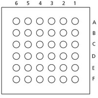
... Package Pin Assignments 36-Pin UC 6 Note: This is the bottom view of the package. Note For Package Manufacturing and Environmental information, visit the Resource Center at http://www.actel.com/products/solutions/package/docs.aspx. IGLOO nano Low Power Flash FPGAs Pin 1 Pad Corner ...
Page 104
Package Pin Assignments 36-Pin UC AGLN010 Pin Number Function A1 IO21RSB1 A2 IO18RSB1 A3 IO13RSB1 A4 GDC0/IO00RSB0 A5 IO06RSB0 A6 GDA0/IO04RSB0 B1 GEC0/IO37RSB1 B2 IO20RSB1 B3 IO15RSB1 B4 IO09RSB0 B5 IO08RSB0 B6 IO07RSB0 C1 IO22RSB1 C2 GEA0/IO34RSB1 C3 GND C4 ...
Page 105
... UC 9 Note: This is the bottom view of the package. Note For Package Manufacturing and Environmental information, visit the Resource Center at http://www.actel.com/products/solutions/package/docs.aspx. A1 Ball Pad Corner IGLOO nano Low Power Flash FPGAs ...
Page 106
Package Pin Assignments 81-Pin UC Pin Number AGLN020 Function A1 IO64RSB2 A2 IO54RSB2 A3 IO57RSB2 A4 IO36RSB1 A5 IO32RSB1 A6 IO24RSB1 A7 IO20RSB1 A8 IO04RSB0 A9 IO08RSB0 B1 IO59RSB2 B2 IO55RSB2 B3 IO62RSB2 B4 IO34RSB1 B5 IO28RSB1 B6 IO22RSB1 B7 ...
Page 107
UC AGLN030Z Pin Number Function A1 IO00RSB0 A2 IO02RSB0 A3 IO06RSB0 A4 IO11RSB0 A5 IO16RSB0 A6 IO19RSB0 A7 IO22RSB0 A8 IO24RSB0 A9 IO26RSB0 B1 IO81RSB1 B2 IO04RSB0 B3 IO10RSB0 B4 IO13RSB0 B5 IO15RSB0 B6 IO20RSB0 B7 IO21RSB0 B8 IO28RSB0 ...
Page 108
... Package Pin Assignments 81-Pin CS Note: This is the bottom view of the package. Note For Package Manufacturing and Environmental information, visit the Resource Center at http://www.actel.com/products/solutions/package/docs.aspx Ball Pad Corner isio ...
Page 109
CS Pin Number AGLN020 Function A1 IO64RSB2 A2 IO54RSB2 A3 IO57RSB2 A4 IO36RSB1 A5 IO32RSB1 A6 IO24RSB1 A7 IO20RSB1 A8 IO04RSB0 A9 IO08RSB0 B1 IO59RSB2 B2 IO55RSB2 B3 IO62RSB2 B4 IO34RSB1 B5 IO28RSB1 B6 IO22RSB1 B7 IO18RSB1 B8 IO00RSB0 ...
Page 110
Package Pin Assignments 81-Pin CS AGLN030Z Pin Number Function A1 IO00RSB0 A2 IO02RSB0 A3 IO06RSB0 A4 IO11RSB0 A5 IO16RSB0 A6 IO19RSB0 A7 IO22RSB0 A8 IO24RSB0 A9 IO26RSB0 B1 IO81RSB1 B2 IO04RSB0 B3 IO10RSB0 B4 IO13RSB0 B5 IO15RSB0 B6 IO20RSB0 B7 ...
Page 111
CS Pin Number AGLN060 Function A1 GAA0/IO02RSB0 A2 GAA1/IO03RSB0 A3 GAC0/IO06RSB0 A4 IO09RSB0 A5 IO13RSB0 A6 IO18RSB0 A7 GBB0/IO21RSB0 A8 GBA1/IO24RSB0 A9 GBA2/IO25RSB0 B1 GAA2/IO95RSB1 B2 GAB0/IO04RSB0 B3 GAC1/IO07RSB0 B4 IO08RSB0 B5 IO15RSB0 B6 GBC0/IO19RSB0 B7 GBB1/IO22RSB0 B8 IO26RSB0 ...
Page 112
Package Pin Assignments 81-Pin CS Pin Number AGLN060Z Function A1 GAA0/IO02RSB0 A2 GAA1/IO03RSB0 A3 GAC0/IO06RSB0 A4 IO09RSB0 A5 IO13RSB0 A6 IO18RSB0 A7 GBB0/IO21RSB0 A8 GBA1/IO24RSB0 A9 GBA2/IO25RSB0 B1 GAA2/IO95RSB1 B2 GAB0/IO04RSB0 B3 GAC1/IO07RSB0 B4 IO08RSB0 B5 IO15RSB0 B6 GBC0/IO19RSB0 B7 ...
Page 113
CS Pin Number AGLN125 Function A1 GAA0/IO00RSB0 A2 GAA1/IO01RSB0 A3 GAC0/IO04RSB0 A4 IO13RSB0 A5 IO22RSB0 A6 IO32RSB0 A7 GBB0/IO37RSB0 A8 GBA1/IO40RSB0 A9 GBA2/IO41RSB0 B1 GAA2/IO132RSB1 B2 GAB0/IO02RSB0 B3 GAC1/IO05RSB0 B4 IO11RSB0 B5 IO25RSB0 B6 GBC0/IO35RSB0 B7 GBB1/IO38RSB0 B8 IO42RSB0 ...
Page 114
Package Pin Assignments 81-Pin CS Pin Number AGLN125Z Function A1 GAA0/IO00RSB0 A2 GAA1/IO01RSB0 A3 GAC0/IO04RSB0 A4 IO13RSB0 A5 IO22RSB0 A6 IO32RSB0 A7 GBB0/IO37RSB0 A8 GBA1/IO40RSB0 A9 GBA2/IO41RSB0 B1 GAA2/IO132RSB1 B2 GAB0/IO02RSB0 B3 GAC1/IO05RSB0 B4 IO11RSB0 B5 IO25RSB0 B6 GBC0/IO35RSB0 B7 ...
Page 115
CS Pin Number AGLN250 Function A1 GAA0/IO00RSB0 A2 GAA1/IO01RSB0 A3 GAC0/IO04RSB0 A4 IO13RSB0 A5 IO21RSB0 A6 IO27RSB0 A7 GBB0/IO37RSB0 A8 GBA1/IO40RSB0 A9 GBA2/IO41PPB1 B1 GAA2/IO118UPB3 B2 GAB0/IO02RSB0 B3 GAC1/IO05RSB0 B4 IO11RSB0 B5 IO23RSB0 B6 GBC0/IO35RSB0 B7 GBB1/IO38RSB0 B8 IO41NPB1 ...
Page 116
Package Pin Assignments 81-Pin CS Pin Number AGLN250Z Function A1 GAA0/IO00RSB0 A2 GAA1/IO01RSB0 A3 GAC0/IO04RSB0 A4 IO07RSB0 A5 IO09RSB0 A6 IO12RSB0 A7 GBB0/IO16RSB0 A8 GBA1/IO19RSB0 A9 GBA2/IO20RSB1 B1 GAA2/IO67RSB3 B2 GAB0/IO02RSB0 B3 GAC1/IO05RSB0 B4 IO06RSB0 B5 IO10RSB0 B6 GBC0/IO14RSB0 B7 ...
Page 117
... QFN Notes: 1. This is the bottom view of the package. 2. The die attach paddle of the package is tied to ground (GND). Note For Package Manufacturing and Environmental information, visit the Resource Center at http://www.actel.com/products/solutions/package/docs.aspx. IGLOO nano Low Power Flash FPGAs Pin ...
Page 118
Package Pin Assignments 48-Pin QFN AGLN010 Pin Number Function 1 GEC0/IO37RSB1 2 IO36RSB1 3 GEA0/IO34RSB1 4 IO22RSB1 5 GND 6 VCCIB1 7 IO24RSB1 8 IO33RSB1 9 IO26RSB1 10 IO32RSB1 11 IO27RSB1 12 IO29RSB1 13 IO30RSB1 14 FF/IO31RSB1 15 IO28RSB1 16 ...
Page 119
QFN Pin Number AGLN030Z Function 1 IO82RSB1 2 GEC0/IO73RSB1 3 GEA0/IO72RSB1 4 GEB0/IO71RSB1 5 GND 6 VCCIB1 7 IO68RSB1 8 IO67RSB1 9 IO66RSB1 10 IO65RSB1 11 IO64RSB1 12 IO62RSB1 13 IO61RSB1 14 FF/IO60RSB1 15 IO57RSB1 16 IO55RSB1 17 IO53RSB1 ...
Page 120
... Package Pin Assignments 68-Pin QFN Notes: 1. This is the bottom view of the package. 2. The die attach paddle of the package is tied to ground (GND). Note For Package Manufacturing and Environmental information, visit the Resource Center at http://www.actel.com/products/solutions/package/docs.aspx Pin A1 Mark sio ...
Page 121
QFN AGLN015 Pin Number Function 1 IO60RSB2 2 IO54RSB2 3 IO52RSB2 4 IO50RSB2 5 IO49RSB2 6 GEC0/IO48RSB2 7 GEA0/IO47RSB2 8 VCC 9 GND 10 VCCIB2 11 IO46RSB2 12 IO45RSB2 13 IO44RSB2 14 IO43RSB2 15 IO42RSB2 16 IO41RSB2 17 IO40RSB2 ...
Page 122
Package Pin Assignments 68-Pin QFN AGLN020 Pin Number Function 1 IO60RSB2 2 IO54RSB2 3 IO52RSB2 4 IO50RSB2 5 IO49RSB2 6 GEC0/IO48RSB2 7 GEA0/IO47RSB2 8 VCC 9 GND 10 VCCIB2 11 IO46RSB2 12 IO45RSB2 13 IO44RSB2 14 IO43RSB2 15 IO42RSB2 16 ...
Page 123
QFN AGLN030Z Pin Number Function 1 IO82RSB1 2 IO80RSB1 3 IO78RSB1 4 IO76RSB1 5 GEC0/IO73RSB1 6 GEA0/IO72RSB1 7 GEB0/IO71RSB1 8 VCC 9 GND 10 VCCIB1 11 IO68RSB1 12 IO67RSB1 13 IO66RSB1 14 IO65RSB1 15 IO64RSB1 16 IO63RSB1 17 IO62RSB1 ...
Page 124
... Package Pin Assignments 100-Pin VQFP 100 1 Note: This is the top view of the package. Note For Package Manufacturing and Environmental information, visit the Resource Center at http://www.actel.com/products/solutions/package/docs.aspx sio ...
Page 125
VQFP AGLN030Z Pin Number Function 1 GND 2 IO82RSB1 3 IO81RSB1 4 IO80RSB1 5 IO79RSB1 6 IO78RSB1 7 IO77RSB1 8 IO76RSB1 9 GND 10 IO75RSB1 11 IO74RSB1 12 GEC0/IO73RSB1 13 GEA0/IO72RSB1 14 GEB0/IO71RSB1 15 IO70RSB1 16 IO69RSB1 17 VCC ...
Page 126
Package Pin Assignments 100-Pin VQFP Pin Number AGLN060 Function 1 GND 2 GAA2/IO51RSB1 3 IO52RSB1 4 GAB2/IO53RSB1 5 IO95RSB1 6 GAC2/IO94RSB1 7 IO93RSB1 8 IO92RSB1 9 GND 10 GFB1/IO87RSB1 11 GFB0/IO86RSB1 12 VCOMPLF 13 GFA0/IO85RSB1 14 VCCPLF 15 GFA1/IO84RSB1 16 ...
Page 127
VQFP Pin Number AGLN060Z Function 1 GND 2 GAA2/IO51RSB1 3 IO52RSB1 4 GAB2/IO53RSB1 5 IO95RSB1 6 GAC2/IO94RSB1 7 IO93RSB1 8 IO92RSB1 9 GND 10 GFB1/IO87RSB1 11 GFB0/IO86RSB1 12 VCOMPLF 13 GFA0/IO85RSB1 14 VCCPLF 15 GFA1/IO84RSB1 16 GFA2/IO83RSB1 17 VCC ...
Page 128
Package Pin Assignments 100-Pin VQFP Pin Number AGLN125 Function 1 GND 2 GAA2/IO67RSB1 3 IO68RSB1 4 GAB2/IO69RSB1 5 IO132RSB1 6 GAC2/IO131RSB1 7 IO130RSB1 8 IO129RSB1 9 GND 10 GFB1/IO124RSB1 11 GFB0/IO123RSB1 12 VCOMPLF 13 GFA0/IO122RSB1 14 VCCPLF 15 GFA1/IO121RSB1 16 ...
Page 129
VQFP Pin Number AGLN125Z Function 1 GND 2 GAA2/IO67RSB1 3 IO68RSB1 4 GAB2/IO69RSB1 5 IO132RSB1 6 GAC2/IO131RSB1 7 IO130RSB1 8 IO129RSB1 9 GND 10 GFB1/IO124RSB1 11 GFB0/IO123RSB1 12 VCOMPLF 13 GFA0/IO122RSB1 14 VCCPLF 15 GFA1/IO121RSB1 16 GFA2/IO120RSB1 17 VCC ...
Page 130
Package Pin Assignments 100-Pin VQFP Pin Number AGLN250 Function 1 GND 2 GAA2/IO67RSB3 3 IO66RSB3 4 GAB2/IO65RSB3 5 IO64RSB3 6 GAC2/IO63RSB3 7 IO62RSB3 8 IO61RSB3 9 GND 10 GFB1/IO60RSB3 11 GFB0/IO59RSB3 12 VCOMPLF 13 GFA0/IO57RSB3 14 VCCPLF 15 GFA1/IO58RSB3 16 ...
Page 131
VQFP Pin Number AGLN250Z Function 1 GND 2 GAA2/IO67RSB3 3 IO66RSB3 4 GAB2/IO65RSB3 5 IO64RSB3 6 GAC2/IO63RSB3 7 IO62RSB3 8 IO61RSB3 9 GND 10 GFB1/IO60RSB3 11 GFB0/IO59RSB3 12 VCOMPLF 13 GFA0/IO57RSB3 14 VCCPLF 15 GFA1/IO58RSB3 16 GFA2/IO56RSB3 17 VCC ...
Page 132
...
Page 133
Datasheet Information List of Changes The following table lists critical changes that were made in each version of the IGLOO nano datasheet. Revision Revision 11 (Jul 2010) The status of the AGLN060 device has changed from Advance to ...
Page 134
Datasheet Information Revision Revision 10 (cont’d) The note stating what was included in I Quiescent Supply Current (IDD) Characteristics, IGLOO nano Shutdown The note, "per VCCI or VJTAG bank" was removed from Supply Current (IDD), No IGLOO nano Flash*Freeze was ...
Page 135
Revision Revision 10 (cont’d) The AGLN250 function for pin C8 in the 22134). Revision 9 (Mar2010) All product tables and pin tables were updated to show clearly that AGLN030 is available only in the Z feature grade at this time. ...
Page 136
Datasheet Information Revision Revision 3 (cont’d) The "81-Pin UC" Packaging Advance The "81-Pin CS" v0.4 Revision 2 (Dec 2008) The second table note in "AGLN060, AGLN125, and AGLN250 in the CS81 package do not support PLLs. Product Brief Advance AGLN030 ...
Page 137
Revision Revision 1 (cont’d) The "48-Pin QFN" Note 2 for the changed to "The die attach paddle of the package is tied to ground (GND)." The "100-Pin VQFP" corner instead of the upper right corner. Revision 0 (Oct 2008) The ...
Page 138
... Actel may amend or enhance products during the product introduction and qualification process, resulting in changes in device functionality or performance the responsibility of each customer to ensure the fitness of any Actel product (but especially a new product) for a particular purpose, including appropriateness for safety-critical, life-support, and other high-reliability applications. ...
Page 139
...
Page 140
... Fax +44 (0) 1276 607 540 © Actel Corporation. All rights reserved. Actel, Actel Fusion, IGLOO, Libero, Pigeon Point, ProASIC, SmartFusion and the associated logos are trademarks or registered trademarks of Actel Corporation. All other trademarks and service marks are the property of their respective owners. ...