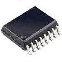
DG403DY-E3 Vishay, DG403DY-E3 Datasheet

DG403DY-E3
Specifications of DG403DY-E3
Related parts for DG403DY-E3
DG403DY-E3 Summary of contents
Page 1
... DG401 series is ON ideally suited for portable and battery powered industrial and military applications. Built on the Vishay Siliconix proprietary high-voltage silicon-gate process to achieve high voltage rating and superior switch on/off performance, break-before-make is guaranteed for the SPDT configurations. An epitaxial layer prevents latchup ...
Page 2
... DG401, DG403, DG405 Vishay Siliconix FUNCTIONAL BLOCK DIAGRAM AND PIN CONFIGURATION DG403 Dual-In-Line and SOIC Key GND Top View DG405 Dual-In-Line and SOIC Key GND Top View www.vishay.com 2 DG403 LCC GND Top View DG405 LCC GND Top View Two SPDT Switches per Package ...
Page 3
... Plastic DIP 16-Pin Plastic DIP c d DG401, DG403, DG405 Vishay Siliconix Part Number DG401DJ DG401DJ-E3 DG401DY DG401DY-T1 DG401DY-E3 DG401DY-T1-E3 DG403DJ DG403DJ-E3 DG403DY DG403DY-E3 DG403DY-T1 DG403DY-T1-E3 DG405DJ DG405DJ-E3 DG405DY DG405DY-E3 DG405DY-T1 DG405DY-T1-E3 Limit 44 25 (GND - 0.3) to (V+) + 0 mA, whichever occurs first 30 ...
Page 4
... DG401, DG403, DG405 Vishay Siliconix a SPECIFICATIONS Parameter Symbol Analog Switch e V Analog Signal Range ANALOG Drain-Source R DS(on) On-Resistance Δ Drain-Source ΔR DS(on) On-Resistance I S(off) Switch Off Leakage Current I D(off) I Channel On Leakage Current D(on) Digital Control Input Current V Low IN Input Current V High ...
Page 5
... D 100 ° 7 Drain Voltage ( vs. V and Power Supply Voltage ( DS(on) D Document Number: 70049 S09-2561-Rev. I, 30-Nov-09 SW1, 2 SW3 DG401, DG403, DG405 Vishay Siliconix 3 (V+) Input Switching Threshold vs. Supply Voltages ° ± ± ± ± ± ± Drain Voltage ( vs. V and Power Supply Voltage ...
Page 6
... DG401, DG403, DG405 Vishay Siliconix TYPICAL CHARACTERISTICS 25 °C, unless otherwise noted 1000p - ± 100p I D (on) 10p I D (off Temperature (°C) Leakage Current vs. Temperature 100 100 Temperature (°C) A Supply Current vs. Temperature 180 160 140 120 100 ± 5 ± 10 ± 15 V+, V- Positive and Negative Supplies (V) Switching Time vs ...
Page 7
... TYPICAL CHARACTERISTICS 25 °C, unless otherwise noted SCHEMATIC DIAGRAM Typical Channel GND V– Document Number: 70049 S09-2561-Rev. I, 30-Nov-09 100 100 µA 10 µA 1 µA 100 100 1K 10K 100K Frequency (Hz) Supply Current vs. Switching Frequency Level Shift/ Drive Figure 1. DG401, DG403, DG405 Vishay Siliconix 1M 10M S V– www.vishay.com 7 ...
Page 8
... DG401, DG403, DG405 Vishay Siliconix TEST CIRCUITS V is the steady state output with the switch on. Feedthrough via switch capacitance may result in spikes at the leading and O trailing edge of the output waveform ± GND - (includes fixture and stray capacitance DS(on GND - (includes fixture and stray capacitance) ...
Page 9
... Ω 2.4 V GND - bypass Figure 6. Insertion Loss Document Number: 70049 S09-2561-Rev. I, 30-Nov- Ω 100 2.4 V Ω 100 V- C DG401, DG403, DG405 Vishay Siliconix + Ω 0.8 V GND Isolation = 20 log TALK bypass Figure 7. Crosstalk + GND Figure 8. Capacitances www.vishay.com C Ω Meter HP4192A Impedance Analyzer ...
Page 10
... DG401, DG403, DG405 Vishay Siliconix APPLICATIONS + Left S Source 1 3 Right IN 1 Left S 2 Source 2 S Right TTL Channel GND Select Figure 9. Stereo Source Selector Dual Slope Integrators: The DG403 is well suited to configure a selectable slope integrator. One control signal selects the timing capacitor ...
Page 11
... A – Vishay Siliconix maintains worldwide manufacturing capability. Products may be manufactured at one of several qualified locations. Reliability data for Silicon Technology and Package Reliability represent a composite of all qualified locations. For related documents such as package/tape drawings, part marking, and reliability data, see www.vishay.com/ppg?70049. ...
Page 12
... Vishay product could result in personal injury or death. Customers using or selling Vishay products not expressly indicated for use in such applications their own risk and agree to fully indemnify and hold Vishay and its distributors harmless from and against any and all claims, liabilities, expenses and damages arising or resulting in connection with such use or sale, including attorneys fees, even if such claim alleges that Vishay or its distributor was negligent regarding the design or manufacture of the part ...


