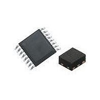
DG211BDJ-E3 Vishay, DG211BDJ-E3 Datasheet - Page 6

DG211BDJ-E3
Manufacturer Part Number
DG211BDJ-E3
Description
Analog Switch ICs Quad SPST Switch
Manufacturer
Vishay
Type
Analog Switchr
Specifications of DG211BDJ-E3
Number Of Switches
Quad
Switch Configuration
SPST
On Resistance (max)
160 Ohms
On Time (max)
300 ns
Off Time (max)
200 ns
Supply Voltage (max)
25 V
Supply Voltage (min)
4.5 V
Maximum Power Dissipation
470 mW
Maximum Operating Temperature
+ 85 C
Mounting Style
Through Hole
Package / Case
PDIP-16
Minimum Operating Temperature
- 40 C
Analog Switch Type
SPST
No. Of Channels
4
On State Resistance Max
45ohm
Turn Off Time
200ns
Turn On Time
300ns
Supply Voltage Range
4.5V To 25V
Operating Temperature Range
-40°C To +85°C
Multiplexer Configuration
Quad SPST
Number Of Inputs
4
Number Of Outputs
4
Number Of Channels
4
Analog Switch On Resistance
160@12VOhm
Package Type
PDIP
Power Supply Requirement
Single/Dual
Single Supply Voltage (min)
4.5V
Single Supply Voltage (typ)
5/9/12/15/18/24V
Single Supply Voltage (max)
25V
Dual Supply Voltage (min)
±4.5V
Dual Supply Voltage (typ)
±5/±9/±12/±15V
Dual Supply Voltage (max)
±22V
Power Dissipation
470mW
Mounting
Through Hole
Pin Count
16
Operating Temp Range
-40C to 85C
Operating Temperature Classification
Industrial
Lead Free Status / RoHS Status
Lead free / RoHS Compliant
Lead Free Status / RoHS Status
Lead free / RoHS Compliant, Lead free / RoHS Compliant
DG211B, DG212B
Vishay Siliconix
TEST CIRCUITS
www.vishay.com
6
V
S
= + 2 V
V
V
3 V
S
g
Off Isolation = 20 log
R
g
0V, 2.4 V
= 50 Ω
3 V
R
g
S
IN
GND
Figure 3. Off Isolation
C
S
IN
+ 15 V
GND
IN
S
V+
V
V
GND
S
O
- 15 V
V+
V-
V
+ 15 V
O
V+
D
+ 15 V
= V
- 15 V
V-
S
- 15 V
V-
D
R
D
R
1 kΩ
L
L
+ r
C
R
DS(on)
L
C
1000 pF
Figure 5. Charge Injection
Figure 2. Switching Time
L
C
35 pF
L
V
R
V
O
L
O
V
O
X
C = RF bypass
TALK
V
Isolation = 20 log
S
Output
Switch
Logic
Input
R
g
Figure 4. Channel-to-Channel Crosstalk
The charge injection in coulombs is Q = C
ΔV
= 50
0 V, 2.4 V
0 V, 2.4 V
O
V
= measured voltage error due to charge injection
3 V
0 V
Ω
O
NC
V
IN
O
X
V
V
C
S
O
ON
S
IN
S
IN
1
2
t
1
2
ON
GND
50 %
V+
90 %
S11-0179-Rev. J, 07-Feb-11
ΔV
OFF
+ 15 V
Document Number: 70040
O
- 15 V
V-
D
D
t
OFF
1
2
L
x ΔV
C
ON
t
t
O
r
f
< 20 ns
< 20 ns
50
R
V
L
O
Ω


