NTE222 NTE ELECTRONICS, NTE222 Datasheet
NTE222
Manufacturer Part Number
NTE222
Description
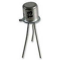
Replacement Semiconductors TO-72 N-CH MOSFET AM
Manufacturer
NTE ELECTRONICS
Datasheet
1.NTE222.pdf
(2 pages)
Specifications of NTE222
Transistor Polarity
N Channel
Continuous Drain Current Id
50mA
Drain Source Voltage Vds
25V
Power Dissipation Pd
360mW
Operating Temperature Range
-65°C To +175°C
No. Of Pins
4
Lead Free Status / RoHS Status
Lead free / RoHS Compliant
Lead Free Status / RoHS Status
Lead free / RoHS Compliant


Absolute Maximum Ratings:
Drain–Source Voltage, V
Drain–Gate Voltage, V
Drain Current, I
Reverse Gate Current, I
Forward Gate Current, I
Total Device Dissipation (T
Total Device Dissipation (T
Operating Junction Temperature Range, T
Storage Temperature Range, T
Lead Temperature (During Soldering), T
Electrical Characteristics: (T
Note 1. All gated breakdown voltages are measured while the device is conducting rated gate cur-
Note 2. Pulse Test: Pulse Width = 30 s, Duty Cycle
Note 3. This parameter must be measured with bias voltages applied for less than five (5) seconds
OFF Characteristics
Drain–Source Breakdown Voltage
Gate 1–Source Breakdown Voltage
Gate 2–Source Breakdown Voltage
Gate 1 Leakage Current
Gate 2 Leakage Current
Gate 1 to Source Cutoff Voltage
Gate 2 to Source Cutoff Voltage
ON Characteristics (Note 2)
Zero–Gate–Voltage Drain Current
Small–Signal Characteristics
Forward Transfer Admittance
Derate Above 25 C
Derate Above 25 C
rent. This insures that the gate voltage limiting network is functioning properly.
to avoid overheating.
Parameter
D
. . . . . . . . . . . . . . . . . . . . . . . . . . . . . . . . . . . . . . . . . . . . . . . . . . . . . . . . . . . . . . . . .
DG
GF
G
DS
. . . . . . . . . . . . . . . . . . . . . . . . . . . . . . . . . . . . . . . . . . . . . . . . . . . . . . . . . . . .
. . . . . . . . . . . . . . . . . . . . . . . . . . . . . . . . . . . . . . . . . . . . . . . . . . . . . . . . .
A
C
. . . . . . . . . . . . . . . . . . . . . . . . . . . . . . . . . . . . . . . . . . . . . . . . . . . . . . . . .
. . . . . . . . . . . . . . . . . . . . . . . . . . . . . . . . . . . . . . . . . . . . . . . . . . . . .
. . . . . . . . . . . . . . . . . . . . . . . . . . . . . . . . . . . . . . . . . . . . . . . . . . . . .
Dual Gate N–Channel MOSFET
. . . . . . . . . . . . . . . . . . . . . . . . . . . . . . . . . . . . . . . . . . . . . . . . . . . . . . . . . .
= +25 C), P
= +25 C), P
stg
A
V
V
= +25 C unless otherwise specified)
V
Field Effect Transistor
Symbol
V
V
(BR)G1SO
(BR)G2SO
(BR)DSX
I
I
G1S(off)
G2S(off)
. . . . . . . . . . . . . . . . . . . . . . . . . . . . . . . . . . . . . . . . . .
G1SS
G2SS
I
|Y
DSS
fs
|
L
D
D
. . . . . . . . . . . . . . . . . . . . . . . . . . . . . . . . . . . . . . . . . . .
J
I
I
I
V
V
V
V
V
V
f = 1kHz, Note 3
D
G1
G2
. . . . . . . . . . . . . . . . . . . . . . . . . . . . . . . . . . . . . . . . .
. . . . . . . . . . . . . . . . . . . . . . . . . . . . . . . . . . . . . . . . . .
G1S
G2S
DS
DS
DS
DS
NTE222
. . . . . . . . . . . . . . . . . . . . . . . . . . . . . . . . . .
= 10 A, V
= 10mA, Note 1
= 10mA, Note 1
= 15V, V
= 15V, V
= 15V, V
= 15V, V
= 5V, V
= 5V, V
Test Conditions
G1
G2S
G1S
G2S
G2S
G2S
G1S
= V
2%.
= 4V, I
= 0V, I
= 4V, V
= 4V, V
= V
= V
G2
DS
DS
= –5V
D
D
G1S
G1S
= 0
= 0
= 20 A
= 20 A
= 0V
= 0V,
–0.5
–0.2
Min
25
10
–
–
6
6
6
Typ
–
–
–
–
–
–
–
–
–
–65 to +175 C
–65 to +175 C
Max
–4.0
–4.0
30
22
–
30
30
10
10
2.4mW/ C
0.8mW/ C
360mW
+300 C
–10mA
1.2mW
mmhos
50mA
10mA
Unit
mA
nA
nA
V
V
V
V
V
25V
30V
Related parts for NTE222
Image
Part Number
Description
Manufacturer
Datasheet
Request
R

Part Number:
Description:
TRANSISTOR,BJT,NPN,80V V(BR)CEO,2A I(C),SIP
Manufacturer:
NTE ELECTRONICS
Datasheet:

Part Number:
Description:
ICS,NTE LED FLASHLIGHTS,ICS,RED TRAFFIC AND SAFETY WAND FOR LW-PRO4000-BLK. MOLDED TRANSLUCENT PLASTIC WAND,TASK LIGHTING,LIGHTWAVE? LED FLASHLIGHTS ,NTE ELECTRONICS
Manufacturer:
NTE ELECTRONICS

Part Number:
Description:
Fuse; Non-Resettable; 15A; Dims 0.16x0.457"; Axial; 120-277VAC; PCB; NTE Series
Manufacturer:
NTE Electronics, Inc.
Datasheet:
Part Number:
Description:
Fuse; Non-Resettable; 15A; Dims 0.16x0.457"; Axial; 120-277VAC; PCB; NTE Series
Manufacturer:
NTE Electronics, Inc.
Datasheet:
Part Number:
Description:
Fuse; Non-Resettable; 15A; Dims 0.16x0.457"; Axial; 120-277VAC; PCB; NTE Series
Manufacturer:
NTE Electronics, Inc.
Datasheet:
Part Number:
Description:
Fuse; Non-Resettable; 15A; Dims 0.16x0.457"; Axial; 120-277VAC; PCB; NTE Series
Manufacturer:
NTE Electronics, Inc.
Datasheet:
Part Number:
Description:
Fuse; Non-Resettable; 15A; Dims 0.16x0.457"; Axial; 120-277VAC; PCB; NTE Series
Manufacturer:
NTE Electronics, Inc.
Datasheet:
Part Number:
Description:
Fuse; Non-Resettable; 15A; Dims 0.16x0.457"; Axial; 120-277VAC; PCB; NTE Series
Manufacturer:
NTE Electronics, Inc.
Datasheet:
Part Number:
Description:
Fuse; Non-Resettable; 15A; Dims 0.16x0.457"; Axial; 120-277VAC; PCB; NTE Series
Manufacturer:
NTE Electronics, Inc.
Datasheet:
Part Number:
Description:
Fuse; Non-Resettable; 15A; Dims 0.16x0.457"; Axial; 120/250VAC; PCB; NTE Series
Manufacturer:
NTE Electronics, Inc.
Datasheet:
Part Number:
Description:
MOTOR START AC ELECTROLYTIC
Manufacturer:
NTE [NTE Electronics]
Datasheet:
Part Number:
Description:
SOLID TANTALUM
Manufacturer:
NTE [NTE Electronics]
Datasheet:
Part Number:
Description:
HIGH-FREQ ALUMINUM ELECTROLYTIC
Manufacturer:
NTE [NTE Electronics]
Datasheet:
Part Number:
Description:
SNAP-IN MOUNT ALUMINUM ELECTROLYTIC
Manufacturer:
NTE [NTE Electronics]
Datasheet:

Part Number:
Description:
Replacement Semiconductors TO-220 NPN PWR AMP
Manufacturer:
NTE ELECTRONICS
Datasheet:
NTE222 Summary of contents
Page 1
... Note 3. This parameter must be measured with bias voltages applied for less than five (5) seconds to avoid overheating. NTE222 Field Effect Transistor . . . . . . . . . . . . . . . . . . . . . . . . . . . . . . . . . . . . . . . . . . . . . . . . . . . . . . . . . . ...
Page 2
Electrical Characteristics (Cont’d): (T Parameter Small–Signal Characteristics (Cont’d) Input Capacitance Reverse Transfer Capacitance Output Capacitance Functional Characteristics Noise Figure Common Source Power Gain Bandwidth Gain Contol Gate–Supply Voltage Note defined as the change Note ...