Description:
The NTE5671 TRIAC is designed for use in applications requiring high bidirectional transient and
blocking voltage capability. Typical applications include AC power control circuits such as lighting, in-
dustrial and domestic heating, motor control and switching systems..
Absolute Maximum Ratings:
Non−Repetitive Peak Off−State Voltage (Either Direction, t ≤ 10ms), V
Repetitive Peak Off−State Voltage (Either Direction, δ ≤ 0.01), V
Crest Working Off−State Voltage (Either Direction), V
RMS On−State Current (Conduction Angle 360°, T
Repetitive Peak On−State Current, I
Non−Repetitive Peak On−State Current, I
I
Rate of Rise of On−State Current After Triggering, dI
Average Power Dissipation (Averaged Over any 20ms Period), P
Peak Power Dissipation, P
RMS Isolation Voltage (From All Three Terminals to External Heatsink[Peak]), V
Isolation Capacitance (From T
Full Operating Temperature, T
Storage Temperature Range, T
Typical Thermal Resistance, Junction−to−Heatsink (See Mounting Instructions), R
Thermal Resistance, Junction−to−Ambient (Note 1), R
Note 1. Mounted on a printed circuit board at any lead length. The quoted value of R
2
t for Fusing (t = 10ms), I
(T
(I
With Heatsink Compound
Without Heatsink Compound
G
used only when no leads of other dissipating components run to the same tie−point.
J
= 200mA to I
= +120°C Prior to Surge, t = 20ms, Full Sine Wave)
T
= 20A, dI
2
t
GM
. . . . . . . . . . . . . . . . . . . . . . . . . . . . . . . . . . . . . . . . . . . . . . . . . . . . . . . .
J
2
. . . . . . . . . . . . . . . . . . . . . . . . . . . . . . . . . . . . . . . . . . . . . . . . . . . . . . .
stg
to External Heatsink), C
. . . . . . . . . . . . . . . . . . . . . . . . . . . . . . . . . . . . . . . . . . . . . . . . . . .
G
. . . . . . . . . . . . . . . . . . . . . . . . . . . . . . . . . . . . . . . . . . . . . . . . . .
. . . . . . . . . . . . . . . . . . . . . . . . . . . . . . . . . . . . . . . . . .
dt = 0.2A/µs)
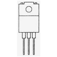
TRIAC − 800V
TRM
. . . . . . . . . . . . . . . . . . . . . . . . . . . . . . . . . . . . . . . . . . . . . . . .
TO220 Full Pack
. . . . . . . . . . . . . . . . . . . . . . . . . . . . . . . . . . . . . . . . . . . . . .
TSM
NTE5671
. . . . . . . . . . . . . . . . . . . . . . . . . . . . . . . . . . . .
H
= +67°C), I
T
RM
DWM
/dt
thJA
(ISO)
, 20A
. . . . . . . . . . . . . . . . . . . . . . . . . . . . . .
. . . . . . . . . . . . . . . . . . . . . . . . . . . .
. . . . . . . . . . . . . . . . . . . . . . . . . . . .
. . . . . . . . . . . . . . . . . . . . . . . . . .
T(RMS)
DRM
G(AV)
. . . . . . . . . . . . . . . . . . . . .
DSM
. . . . . . . . . . . . . . . . . . . .
. . . . . . . . . . . . . . . . . . .
. . . . . . . . . . . . . . . .
(ISO)
thJH
−40° to +125°C
thJA
. . . . . .
should be
+120°C
3.5K/W
4.5K/W
30A/µs
55K/W
1000V
95A
800V
800V
400V
140A
140A
0.5W
5.0W
12pF
16A
2
s