CH0402-250UJNT Vishay, CH0402-250UJNT Datasheet
CH0402-250UJNT
Specifications of CH0402-250UJNT


Related parts for CH0402-250UJNT


CH0402-250UJNT Summary of contents
Page 1
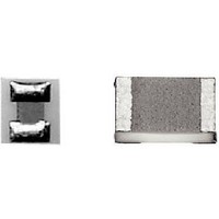
... Note ( 0. Please see document “Vishay Material Category Policy”: www.vishay.com 46 FEATURES • SMD wraparound or flip chip resistor • Small size, down to 20 mils by 16 mils • Edged trimmed block resistors • Pure alumina substrate (99.5 %) • ...
Page 2
... P: “Diameter of true position placement accuracy to the center of land pattern”. For rectangular component Flip-Chip mounting, we suggest min. Z max max. 1.55 0.15 2.37 0.35 For technical questions, contact: sfer@vishay.com Vishay Sfernice X max. G min. 0.15 0.4 0.760 Standard”: (TOE (HELL (SDE min. max. 0.73 ...
Page 3
... Vishay Sfernice highly recommend to use the smallest sizes and flip chip version to get the best performances. Recommended Values: 10R/18R/25R/50R/75R/100R/150R/180R/200R/250R/330R/500R Those values are available with a MOQ of 100 pieces. Other values can be ordered upon request, but higher MOQ will apply: 1000 pieces for CH02016, 500 pieces for CH0402, 250 pieces for CH0603. Recommended terminations: F ...
Page 4
... C – L Cω – 1 θ ------------------------------------------------------------ - = tan The smaller the product the greater the frequency range over --- - = versus frequency. ------- - R and For technical questions, contact: sfer@vishay.com Vishay Sfernice Resistance Cω ω – C – L Cω ------------------------------------------------------------ - will be combined to internal reactance of L and g impedance transmission line ...
Page 5
... CH Vishay Sfernice INTERNAL IMPEDANCE CURVES 1.1 1.0 0.9 0.8 0.7 0.6 0.5 0.4 0.3 0.2 0.1 0.1 1.1 1.0 0.9 0.8 0.7 0.6 0.5 0.4 0.3 0.2 0.1 0.1 www.vishay.com 50 50 GHz Thin Film Microwave Resistors 1 f (GHz) Internal impedance curve for 02016 size (F and P terminations) ...
Page 6
... Revision: 29-Nov- (GHz) Internal impedance curve for 0402 size (N and G terminations (GHz) Internal impedance curve for 0603 size (F and P terminations) For technical questions, contact: sfer@vishay.com Vishay Sfernice 10 Ω 25 Ω 50 Ω 75 Ω 100 Ω 150 Ω 200 Ω 250 Ω 500 Ω ...
Page 7
... CH Vishay Sfernice INTERNAL IMPEDANCE CURVES 1.1 1.0 0.9 0.8 0.7 0.6 0.5 0.4 0.3 0.2 0.1 0.1 S PARAMETER CH02016 (F and P Terminations 0 (GHz) CH02016 flip chip ( www.vishay.com 52 50 GHz Thin Film Microwave Resistors 10 Ω (GHz) Internal impedance curve for 0603 size (N and G terminations) ...
Page 8
... GHz Thin Film Microwave Resistors S PARAMETER CH0402 (F and P Terminations 0 (GHz) CH0402 flip chip ( CH0402 (N and G Terminations 0 (GHz) CH0402 wraparound ( CH0603 (F and P Terminations 0 (GHz) CH0603 flip chip ( Document Number: 53014 Revision: 29-Nov- S21 - S11 - 100 0 Ω S21 - S11 - 100 0 Ω S11 - 5 S21 ...
Page 9
... CH Vishay Sfernice S PARAMETER CH0603 (N and G Terminations 0 (GHz) CH0603 wraparound ( www.vishay.com 54 50 GHz Thin Film Microwave Resistors - 2 S11 - S21 - 100 0 Ω For technical questions, contact: sfer@vishay.com (GHz 100 Ω) CH0603 wraparound ( Document Number: 53014 Revision: 29-Nov-10 S21 S11 100 ...
Page 10
... Vishay product could result in personal injury or death. Customers using or selling Vishay products not expressly indicated for use in such applications their own risk and agree to fully indemnify and hold Vishay and its distributors harmless from and against any and all claims, liabilities, expenses and damages arising or resulting in connection with such use or sale, including attorneys fees, even if such claim alleges that Vishay or its distributor was negligent regarding the design or manufacture of the part ...