CPA550-4530G POWER ONE, CPA550-4530G Datasheet - Page 11
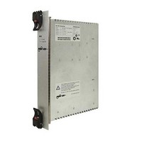
CPA550-4530G
Manufacturer Part Number
CPA550-4530G
Description
DC/DC Converters & Regulators 90-264Vin 550W 5V50A 3.3V50A/12V8A/-12V3A
Manufacturer
POWER ONE
Datasheet
1.CPA250-4530G.pdf
(19 pages)
Specifications of CPA550-4530G
Output Power
550 W
Input Voltage Range
90 V to 264 V
Input Voltage (nominal)
230 V
Number Of Outputs
4
Output Voltage (channel 1)
5 V
Output Current (channel 1)
50 A
Output Voltage (channel 2)
3.3 V
Output Current (channel 2)
50 A
Output Voltage (channel 3)
12 V
Output Current (channel 3)
8 A
Package / Case Size
233.3 mm x 162.5 mm x 40.4 mm
Output Voltage
5 V to 12 V
Lead Free Status / RoHS Status
Lead free / RoHS Compliant


Fig. 8
Degrade signal: NPN output V
Temperature Warning and Shutdown
A temperature warning circuitry monitors the case
temperature T
to low impedance, when the T
level, and changes back to high impedance, when T
below the lower threshold level, which is 85 °C ± 5 °C.
Pin 38 (degrade signal DEG#) is internally connected via the
collector-emitter path of an NPN transistor to the signal
return pin 22. The current I
exceed 40 mA, and V
If T
resumes operation automatically, once T
Fig. 9
Degrade signal V
Power Fail Signal
The power fail circuitry monitors the input voltage V
output voltages. The signal V
impedance (<0.5 V), when one of the monitored voltages
falls below the threshold. V
impedance, when all monitored voltages exceed their
threshold level.
The threshold level for V
V
BCD20005-G Rev. AF, 18-Aug-10
o nom
V
DEG#
C
46
47
10
.
exceeds 105 °C, the converter will be disabled. It
4
8
0
6
2
[V]
60
signal DEG#
C
70
. Its output signal V
DEG#
DEG#
®
versus case temperature T
80
o
should not exceed 40 V.
corresponds to approx. 90% of
DEG#
C
FAL#
DEG#
FAL#
90
exceeds the upper threshold
200 – 550 Watt CompactPCI
11056a
through pin 38 should not
changes from high to low
38
22
changes back to high
DEG#
thermal shutdown
40 V, I
100
Vo+
RTN
DEG#
C
changes from high
falls below 105 °C.
I
DEG#
DEG#
V
DEG#
110
05189c
R
20 mA
C
p
i
°C
and all
C
Page 11 of 19
1
0.8
0.6
0.4
0.2
0
falls
The threshold levels for V
CPD models and 80 – 90 VAC for CPA models.
Connector pin 42 (signal V
the drain-source path of a JFET (self-conducting type) to
the signal return pin 22. The current I
exceed 10 mA. V
not protected against overvoltage.
Fig.10
Power Fail: JFET output, I
Sense Lines
This feature is available only for the outputs Vo1, Vo2, Vo3,
and allows the compensation of voltage drops across the
connector contacts and if necessary, across the load lines.
To ensure correct operation, all sense lines S+ (Vo1SENSE,
Vo2SENSE, and Vo3SENSE) should be connected to the
respective power outputs. The common sense return S–
(SRTN) should be connected to RTN (pin 5 – 12).
The voltage difference between any sense line at its
respective power output pin (as measured on the
connector) should not exceed the following values.
Table 7: Sense line data
Output
Note: CPD200/250 (and CPA200/250 up to version V116)
provide only the signal FAL#, but the converter is not
inhibited.
Note: V
V
Note: Open sense lines are admissible, but the output
voltage regulation will be poor.
Note: If the sense lines S+ and S– compensate for a
considerable voltage drop, the output loads shall be reduced
in order to respect the maximum output power.
i
[V]
3.3
12
5
remains for typ. 30 ms below
47
46
i min
®
of CPA models is considered as insufficient, when
AC-DC and DC-DC Converters
Total voltage difference between sense lines
and their respective outputs
CPA, CPD Series Data Sheet
FAL#
should not exceed 40 V, as the JFET is
FAL#
i
FAL#
correspond to approx. 34 V for
0.8 V
1 V
1 V
) is internally connected via
–
10 mA
2 • V
11006c
42
22
i min
FAL#
RTN
Vo+
.
www.power-one.com
I
FAL#
FAL#
V
FAL#
should not
R
p
Related parts for CPA550-4530G
Image
Part Number
Description
Manufacturer
Datasheet
Request
R

Part Number:
Description:
SWITCHING POWER SUPPLIES, SINGLE OUTPUT, 80 WATTS
Manufacturer:
POWER ONE
Datasheet:
Part Number:
Description:
HAS SERIES - 30 WATT
Manufacturer:
POWER ONE
Datasheet:
Part Number:
Description:
SINGLE OUTPUT
Manufacturer:
POWER ONE
Datasheet:

Part Number:
Description:
BRS DC/DC converters(1.5 WATT)
Manufacturer:
Power-One
Datasheet:
Part Number:
Description:
3...15 Watt DC-DC Converter
Manufacturer:
Power-One
Datasheet:
Part Number:
Description:
HBS SERIES - 100 WATT
Manufacturer:
Power-One
Datasheet:
Part Number:
Description:
3...15 Watt DC-DC Converter
Manufacturer:
Power-One
Datasheet:
Part Number:
Description:
BUS DC/DC converters(3 WATT)
Manufacturer:
Power-One
Datasheet:
Part Number:
Description:
HES SERIES 150 WATT
Manufacturer:
Power-One
Datasheet:
Part Number:
Description:
1.25 WATT
Manufacturer:
Power-One
Datasheet: