CPD500-4530G POWER ONE, CPD500-4530G Datasheet - Page 10

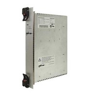
CPD500-4530G
Manufacturer Part Number
CPD500-4530G
Description
DC/DC Converters & Regulators 36-75Vin 500W 5V40A 3.3V50A/12V8A/-12V3A
Manufacturer
POWER ONE
Datasheet
1.CPA250-4530G.pdf
(19 pages)
Specifications of CPD500-4530G
Output Power
500 W
Input Voltage Range
36 V to 75 V
Input Voltage (nominal)
48 V
Number Of Outputs
4
Output Voltage (channel 1)
5 V
Output Current (channel 1)
40 A
Output Voltage (channel 2)
3.3 V
Output Current (channel 2)
50 A
Output Voltage (channel 3)
12 V
Output Current (channel 3)
8 A
Package / Case Size
162.5 mm x 100 mm x 40.6 mm
Output Voltage
5 V to 12 V
Lead Free Status / RoHS Status
Lead free / RoHS Compliant
Fig. 4c
Output power versus T
A temperature sensor fitted on the main PCB provides
approx. 20 °C below T
Auxiliary Functions
Inhibit and Enable
The inhibit input INH# enables (logic high) or disables
(logic low, pull down) all outputs, if a logic signal (TTL,
Fig. 6
Inhibit and enable inputs
BCD20005-G Rev. AF, 18-Aug-10
Table 6: Inhibit data
Characteristics
V
t
t
Caution: The installer must ensure that under all operating
conditions T
fig. 4.
Note: Forced-air cooling (or an additional heat sink on
customer-specific models) can improve the reliability or
allow for higher T
shall never be exceeded.
inh
r
f
1.0
0.5
0.6
46
47
P
0
o
T
/P
A min
Inhibit
voltage
Rise time
Fall time
o nom
Convection cooling
in upright position
C
remains within the limits shown in the diagrams
CPA550
V
V
o
A
o
, as shown in the diagrams fig. 4, but T
CPA/CPD500
= off V
= on
JM012a
A
30
®
at V
C max
Conditions
I
o
i min
= 0 – I
300 LFM = 1.5 m/s (CPA/CPD500)
400 LFM = 2 m/s (CPA550)
i nom
INH#
40
EN#
06153d
RTN
– V
a warning signal (DEG#), at
(CPA500/550, CPD500)
200 – 550 Watt CompactPCI
o max
i max
(22)
39
27
50
min
depending on I
2.4
–2
70
typ max Unit
V
INH#
120
0.8
50
90 °C
o
C max
ms
Page 10 of 19
V
which the control logic begins to reduce the output power.
The output power returns to the normal value, when the
temperature drops back below this limit; see Temperature
Warning and Shutdown.
Output Filter
The output ripple voltage can be reduced by an external
filter to less then 5 mV
Fig. 5
Output filter reducing the output ripple of Vo1 and Vo2
CMOS) is applied. In systems consisting of several
converters this feature may be used to control the activation
sequence of the converters by means of logic signals, or to
enable the source to start-up, before full load is applied.
Fig. 7
Typical output response as a function of inhibit voltage.
Pin 27 (EN#) must be connected to a return pin (e.g., pin 22)
to enable the converter. Pin 27 is shorter than the others
ensuring start-up only, when all other pins are already
connected to the system providing true hot-swap capability.
• C1, C2: Low ESR capacitor, e.g., OS-CON 100 – 470 µF
• L1, L2: Choke 1 – 4.7 µH with appropriate rated current,
Note: If this function is not used, the inhibit pin 39 can be left
open-circuit (not connected). If pin 39 is connected to a return
pin (e.g., pin 22), the internal logic will disable all outputs. The
inhibit input is protected by a decoupling diode.
e.g., Coiltronics
V
0.1
o
Inhibit
1
1
0
0
/V
46
47
o nom
®
AC-DC and DC-DC Converters
CPA, CPD Series Data Sheet
®
t
r
HC2LP 1 µH /33 A or 2.2 µH /24 A.
JM010
pp
13 –18
. Recommended values:
5 –12
1 – 4
30
33
Vo2SENSE
Vo1SENSE
Vo1
Vo2
RTN
L
2
C
2
L
+
1
www.power-one.com
t
f
+
06155a
C
1
3.3 V
5 V
Gnd
t
t


