MRFE6VP6300HR3 Freescale Semiconductor, MRFE6VP6300HR3 Datasheet
MRFE6VP6300HR3
Specifications of MRFE6VP6300HR3


Related parts for MRFE6VP6300HR3

MRFE6VP6300HR3 Summary of contents
Page 1
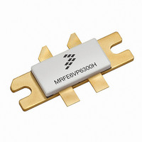
... MRFE6VP6300HSR3 1.8- -600 MHz, 300 LATERAL N- -CHANNEL BROADBAND RF POWER MOSFETs CASE 465M- -01, STYLE 1 NI- -780- -4 MRFE6VP6300HR3 CASE 465H- -02, STYLE 1 NI- -780S- -4 MRFE6VP6300HSR3 out out DS out GS (Top View) Figure 1. Pin Connections (2,3) Symbol Value Unit °C/W Z 0.05 θJC R 0.19 θJC MRFE6VP6300HR3 MRFE6VP6300HSR3 1 ...
Page 2
... Vdc ± 30 mV(rms) MHz Functional Tests (In Freescale Test Fixture, 50 ohm system) V Pulsed, 100 μsec Pulse Width, 20% Duty Cycle Power Gain Drain Efficiency Input Return Loss 1. Each side of device measured separately. MRFE6VP6300HR3 MRFE6VP6300HSR3 2 = 25°C unless otherwise noted) A Symbol I GSS V (BR)DSS ...
Page 3
... Microstrip Z5 0.322″ x 0.220″ Microstrip Z6 0.168″ x 0.220″ Microstrip Z7, Z8 0.282″ x 0.630″ Microstrip Figure 2. MRFE6VP6300HR3(HSR3) Test Circuit Schematic Table 5. MRFE6VP6300HR3(HSR3) Test Circuit Component Designations and Values Part C1, C20 15 pF Chip Capacitors Chip Capacitor C3, C17 91 pF Chip Capacitors ...
Page 4
... Figure 3. MRFE6VP6300HR3(HSR3) Test Circuit Component Layout MRFE6VP6300HR3 MRFE6VP6300HSR3 4 C14 C10 C17 MRFE6VP6300H/HS Rev. 2 C15 C13 C16 C12 C11 C18 C20 C19 RF Device Data Freescale Semiconductor ...
Page 5
... DD 50 100 150 200 250 300 P , OUTPUT POWER (WATTS) PULSED out Figure 7. Pulsed Power Gain versus Output Power = 100 mA 230 MHz 25_C 85_C DQ --30_C G ps 25_C η D 100 P , OUTPUT POWER (WATTS) PULSED out versus Output Power MRFE6VP6300HR3 MRFE6VP6300HSR3 350 400 600 5 ...
Page 6
... DQ 29 1400 mA 28 1100 mA 900 650 Vdc 230 MHz 230.1 MHz DD Two--Tone Measurements OUTPUT POWER (WATTS) PEP out Figure 12. Two- -Tone Power Gain versus Output Power MRFE6VP6300HR3 MRFE6VP6300HSR3 6 -- Two--Tone Measurements --20 --30 --40 --50 --60 --70 400 0.1 -- --20 Two--Tone Measurements -- 650 mA ...
Page 7
... T , JUNCTION TEMPERATURE (°C) J This above graph displays calculated MTTF in hours when the device is operated Vdc 300 W Avg., and η DD out MTTF calculator available at http://www.freescale.com/rf. Select Software & Tools/Development Tools/Calculators to access MTTF calculators by product. 230 250 = 80%. D MRFE6VP6300HR3 MRFE6VP6300HSR3 7 ...
Page 8
... Ω o Input Matching Network Figure 15. Series Equivalent Source and Load Impedance MRFE6VP6300HR3 MRFE6VP6300HSR3 8 Z source f = 230 MHz f = 230 MHz Z load Vdc 100 mA 300 W Peak DD DQ out source load MHz Ω Ω 230 0.65 + j2.79 1.64 + j2. Test circuit impedance as measured from source gate to ground ...
Page 9
... RF Device Data Freescale Semiconductor PACKAGE DIMENSIONS MRFE6VP6300HR3 MRFE6VP6300HSR3 9 ...
Page 10
... MRFE6VP6300HR3 MRFE6VP6300HSR3 10 RF Device Data Freescale Semiconductor ...
Page 11
... RF Device Data Freescale Semiconductor MRFE6VP6300HR3 MRFE6VP6300HSR3 11 ...
Page 12
... MRFE6VP6300HR3 MRFE6VP6300HSR3 12 RF Device Data Freescale Semiconductor ...
Page 13
... For Software Part Number search at http://www.freescale.com, and select the “Part Number” link the Software & Tools tab on the part’s Product Summary page to download the respective tool. The following table summarizes revisions to this document. Revision Date 0 Oct. 2010 • Initial Release of Data Sheet RF Device Data Freescale Semiconductor REVISION HISTORY Description MRFE6VP6300HR3 MRFE6VP6300HSR3 13 ...
Page 14
... For Literature Requests Only: Freescale Semiconductor Literature Distribution Center 1--800--441--2447 or +1--303--675--2140 Fax: +1--303--675--2150 LDCForFreescaleSemiconductor@hibbertgroup.com MRFE6VP6300HR3 MRFE6VP6300HSR3 Document Number: MRFE6VP6300H Rev. 0, 10/2010 14 Information in this document is provided solely to enable system and software implementers to use Freescale Semiconductor products. There are no express or implied copyright licenses granted hereunder to design or fabricate any integrated circuits or integrated circuits based on the information in this document ...