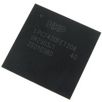
LPC2420FET208,551 NXP Semiconductors, LPC2420FET208,551 Datasheet - Page 11

LPC2420FET208,551
Manufacturer Part Number
LPC2420FET208,551
Description
IC ARM7 MCU 16BIT T208FBGA
Manufacturer
NXP Semiconductors
Series
LPC2400r
Datasheet
1.LPC2460FBD208551.pdf
(79 pages)
Specifications of LPC2420FET208,551
Core Processor
ARM7
Core Size
16/32-Bit
Speed
72MHz
Connectivity
EBI/EMI, I²C, Microwire, MMC, SPI, SSI, SSP, UART/USART, USB OTG
Peripherals
Brown-out Detect/Reset, DMA, I²S, POR, PWM, WDT
Number Of I /o
160
Program Memory Type
ROMless
Ram Size
82K x 8
Voltage - Supply (vcc/vdd)
3 V ~ 3.6 V
Data Converters
A/D 8x10b; D/A 1x10b
Oscillator Type
Internal
Operating Temperature
-40°C ~ 85°C
Package / Case
208-TFBGA
Processor Series
LPC2420
Core
ARM7
Data Bus Width
16 bit, 32 bit
Data Ram Size
98 KB
Interface Type
SPI, I2C, I2S, USB, SSP
Maximum Clock Frequency
72 MHz
Number Of Programmable I/os
160
Number Of Timers
4
Maximum Operating Temperature
+ 85 C
Mounting Style
SMD/SMT
Minimum Operating Temperature
- 40 C
Processor To Be Evaluated
ARM7TDMI-S
Lead Free Status / RoHS Status
Lead free / RoHS Compliant
Program Memory Size
-
Eeprom Size
-
Lead Free Status / Rohs Status
Details
Other names
568-5216
Available stocks
Company
Part Number
Manufacturer
Quantity
Price
Company:
Part Number:
LPC2420FET208,551
Manufacturer:
MAX
Quantity:
65
Company:
Part Number:
LPC2420FET208,551
Manufacturer:
NXP Semiconductors
Quantity:
10 000
NXP Semiconductors
Table 4.
LPC2420_60_5
Preliminary data sheet
Symbol
P0[12]/
USB_PPWR2/
MISO1/AD0[6]
P0[13]/
USB_UP_LED2/
MOSI1/AD0[7]
P0[14]/
USB_HSTEN2/
USB_CONNECT2/
SSEL1
P0[15]/TXD1/
SCK0/SCK
P0[16]/RXD1/
SSEL0/SSEL
P0[17]/CTS1/
MISO0/MISO
P0[18]/DCD1/
MOSI0/MOSI
P0[19]/DSR1/
MCICLK/SDA1
P0[20]/DTR1/
MCICMD/SCL1
Pin description
Pin
41
45
69
128
130
126
124
122
120
[2]
[2]
[1]
[1]
[1]
[1]
[1]
[1]
[1]
…continued
Ball
R1
R2
T7
J16
J14
K17
K15
L17
M17
[1]
[2]
[2]
[1]
[1]
[1]
[1]
[1]
[1]
Type
I/O
O
I/O
I
I/O
O
I/O
I
I/O
O
O
I/O
I/O
O
I/O
I/O
I/O
I
I/O
I/O
I/O
I
I/O
I/O
I/O
I
I/O
I/O
I/O
I
O
I/O
I/O
O
I/O
I/O
Rev. 05 — 24 February 2010
Description
P0[12] — General purpose digital input/output pin.
USB_PPWR2 — Port Power enable signal for USB port 2.
MISO1 — Master In Slave Out for SSP1.
AD0[6] — A/D converter 0, input 6.
P0[13] — General purpose digital input/output pin.
USB_UP_LED2 — USB port 2 GoodLink LED indicator. It is LOW when
device is configured (non-control endpoints enabled). It is HIGH when the
device is not configured or during global suspend.
MOSI1 — Master Out Slave In for SSP1.
AD0[7] — A/D converter 0, input 7.
P0[14] — General purpose digital input/output pin.
USB_HSTEN2 — Host Enabled status for USB port 2.
USB_CONNECT2 — SoftConnect control for USB port 2. Signal used to
switch an external 1.5 kΩ resistor under software control. Used with the
SoftConnect USB feature.
SSEL1 — Slave Select for SSP1.
P0[15] — General purpose digital input/output pin.
TXD1 — Transmitter output for UART1.
SCK0 — Serial clock for SSP0.
SCK — Serial clock for SPI.
P0 [16] — General purpose digital input/output pin.
RXD1 — Receiver input for UART1.
SSEL0 — Slave Select for SSP0.
SSEL — Slave Select for SPI.
P0[17] — General purpose digital input/output pin.
CTS1 — Clear to Send input for UART1.
MISO0 — Master In Slave Out for SSP0.
MISO — Master In Slave Out for SPI.
P0[18] — General purpose digital input/output pin.
DCD1 — Data Carrier Detect input for UART1.
MOSI0 — Master Out Slave In for SSP0.
MOSI — Master Out Slave In for SPI.
P0[19] — General purpose digital input/output pin.
DSR1 — Data Set Ready input for UART1.
MCICLK — Clock output line for SD/MMC interface.
SDA1 — I
P0[20] — General purpose digital input/output pin.
DTR1 — Data Terminal Ready output for UART1.
MCICMD — Command line for SD/MMC interface.
SCL1 — I
2
2
C1 clock input/output (this is not an open-drain pin).
C1 data input/output (this is not an open-drain pin).
Flashless 16-bit/32-bit microcontroller
LPC2420/2460
© NXP B.V. 2010. All rights reserved.
11 of 79


