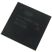
LPC2420FET208,551 NXP Semiconductors, LPC2420FET208,551 Datasheet - Page 29

LPC2420FET208,551
Manufacturer Part Number
LPC2420FET208,551
Description
IC ARM7 MCU 16BIT T208FBGA
Manufacturer
NXP Semiconductors
Series
LPC2400r
Datasheet
1.LPC2460FBD208551.pdf
(79 pages)
Specifications of LPC2420FET208,551
Core Processor
ARM7
Core Size
16/32-Bit
Speed
72MHz
Connectivity
EBI/EMI, I²C, Microwire, MMC, SPI, SSI, SSP, UART/USART, USB OTG
Peripherals
Brown-out Detect/Reset, DMA, I²S, POR, PWM, WDT
Number Of I /o
160
Program Memory Type
ROMless
Ram Size
82K x 8
Voltage - Supply (vcc/vdd)
3 V ~ 3.6 V
Data Converters
A/D 8x10b; D/A 1x10b
Oscillator Type
Internal
Operating Temperature
-40°C ~ 85°C
Package / Case
208-TFBGA
Processor Series
LPC2420
Core
ARM7
Data Bus Width
16 bit, 32 bit
Data Ram Size
98 KB
Interface Type
SPI, I2C, I2S, USB, SSP
Maximum Clock Frequency
72 MHz
Number Of Programmable I/os
160
Number Of Timers
4
Maximum Operating Temperature
+ 85 C
Mounting Style
SMD/SMT
Minimum Operating Temperature
- 40 C
Processor To Be Evaluated
ARM7TDMI-S
Lead Free Status / RoHS Status
Lead free / RoHS Compliant
Program Memory Size
-
Eeprom Size
-
Lead Free Status / Rohs Status
Details
Other names
568-5216
Available stocks
Company
Part Number
Manufacturer
Quantity
Price
Company:
Part Number:
LPC2420FET208,551
Manufacturer:
MAX
Quantity:
65
Company:
Part Number:
LPC2420FET208,551
Manufacturer:
NXP Semiconductors
Quantity:
10 000
NXP Semiconductors
LPC2420_60_5
Preliminary data sheet
7.7.1 Features
7.7 General purpose DMA controller
Note: Synchronous static memory devices (synchronous burst mode) are not supported.
The GPDMA is an AMBA AHB compliant peripheral allowing selected LPC2420/2460
peripherals to have DMA support.
The GPDMA enables peripheral-to-memory, memory-to-peripheral,
peripheral-to-peripheral, and memory-to-memory transactions. Each DMA stream
provides unidirectional serial DMA transfers for a single source and destination. For
example, a bidirectional port requires one stream for transmit and one for receive. The
source and destination areas can each be either a memory region or a peripheral, and
can be accessed through the AHB master.
•
•
•
•
•
•
•
•
•
•
•
•
– Asynchronous page mode read
– Programmable Wait States
– Bus turnaround delay
– Output enable and write enable delays
– Extended wait
Four chip selects for synchronous memory and four chip selects for static memory
devices.
Power-saving modes dynamically control CKE and CLKOUT to SDRAMs.
Dynamic memory self-refresh mode controlled by software.
Controller supports 2048, 4096, and 8192 row address synchronous memory parts.
That is typical 512 MB, 256 MB, and 128 MB parts, with 4, 8, 16, or 32 data bits per
device.
Separate reset domains allow the for auto-refresh through a chip reset if desired.
Two DMA channels. Each channel can support a unidirectional transfer.
The GPDMA can transfer data between the 16 kB SRAM, external memory, and
peripherals such as the SD/MMC, two SSPs, and the I
Single DMA and burst DMA request signals. Each peripheral connected to the
GPDMA can assert either a burst DMA request or a single DMA request. The DMA
burst size is set by programming the GPDMA.
Memory-to-memory, memory-to-peripheral, peripheral-to-memory, and
peripheral-to-peripheral transfers.
Scatter or gather DMA is supported through the use of linked lists. This means that
the source and destination areas do not have to occupy contiguous areas of memory.
Hardware DMA channel priority. Each DMA channel has a specific hardware priority.
DMA channel 0 has the highest priority and channel 1 has the lowest priority. If
requests from two channels become active at the same time, the channel with the
highest priority is serviced first.
AHB slave DMA programming interface. The GPDMA is programmed by writing to the
DMA control registers over the AHB slave interface.
Rev. 05 — 24 February 2010
Flashless 16-bit/32-bit microcontroller
2
LPC2420/2460
S interface.
© NXP B.V. 2010. All rights reserved.
29 of 79


