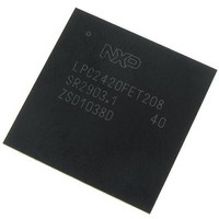
LPC2420FET208,551 NXP Semiconductors, LPC2420FET208,551 Datasheet - Page 30

LPC2420FET208,551
Manufacturer Part Number
LPC2420FET208,551
Description
IC ARM7 MCU 16BIT T208FBGA
Manufacturer
NXP Semiconductors
Series
LPC2400r
Datasheet
1.LPC2460FBD208551.pdf
(79 pages)
Specifications of LPC2420FET208,551
Core Processor
ARM7
Core Size
16/32-Bit
Speed
72MHz
Connectivity
EBI/EMI, I²C, Microwire, MMC, SPI, SSI, SSP, UART/USART, USB OTG
Peripherals
Brown-out Detect/Reset, DMA, I²S, POR, PWM, WDT
Number Of I /o
160
Program Memory Type
ROMless
Ram Size
82K x 8
Voltage - Supply (vcc/vdd)
3 V ~ 3.6 V
Data Converters
A/D 8x10b; D/A 1x10b
Oscillator Type
Internal
Operating Temperature
-40°C ~ 85°C
Package / Case
208-TFBGA
Processor Series
LPC2420
Core
ARM7
Data Bus Width
16 bit, 32 bit
Data Ram Size
98 KB
Interface Type
SPI, I2C, I2S, USB, SSP
Maximum Clock Frequency
72 MHz
Number Of Programmable I/os
160
Number Of Timers
4
Maximum Operating Temperature
+ 85 C
Mounting Style
SMD/SMT
Minimum Operating Temperature
- 40 C
Processor To Be Evaluated
ARM7TDMI-S
Lead Free Status / RoHS Status
Lead free / RoHS Compliant
Program Memory Size
-
Eeprom Size
-
Lead Free Status / Rohs Status
Details
Other names
568-5216
Available stocks
Company
Part Number
Manufacturer
Quantity
Price
Company:
Part Number:
LPC2420FET208,551
Manufacturer:
MAX
Quantity:
65
Company:
Part Number:
LPC2420FET208,551
Manufacturer:
NXP Semiconductors
Quantity:
10 000
NXP Semiconductors
LPC2420_60_5
Preliminary data sheet
7.8.1 Features
7.8 Fast general purpose parallel I/O
Device pins that are not connected to a specific peripheral function are controlled by the
GPIO registers. Pins may be dynamically configured as inputs or outputs. Separate
registers allow setting or clearing any number of outputs simultaneously. The value of the
output register may be read back as well as the current state of the port pins.
LPC2420/2460 use accelerated GPIO functions:
Additionally, any pin on port 0 and port 2 (total of 64 pins) that is not configured as an
analog input/output can be programmed to generate an interrupt on a rising edge, a falling
edge, or both. The edge detection is asynchronous, so it may operate when clocks are not
present such as during Power-down mode. Each enabled interrupt can be used to wake
the chip up from Power-down mode.
•
•
•
•
•
•
•
•
•
•
•
•
•
•
•
•
•
One AHB master for transferring data. This interface transfers data when a DMA
request goes active.
32-bit AHB master bus width.
Incrementing or non-incrementing addressing for source and destination.
Programmable DMA burst size. The DMA burst size can be programmed to more
efficiently transfer data. Usually the burst size is set to half the size of the FIFO in the
peripheral.
Internal four-word FIFO per channel.
Supports 8-bit, 16-bit, and 32-bit wide transactions.
An interrupt to the processor can be generated on a DMA completion or when a DMA
error has occurred.
Interrupt masking. The DMA error and DMA terminal count interrupt requests can be
masked.
Raw interrupt status. The DMA error and DMA count raw interrupt status can be read
prior to masking.
GPIO registers are relocated to the ARM local bus so that the fastest possible I/O
timing can be achieved.
Mask registers allow treating sets of port bits as a group, leaving other bits
unchanged.
All GPIO registers are byte and half-word addressable.
Entire port value can be written in one instruction.
Bit level set and clear registers allow a single instruction to set or clear any number of
bits in one port.
Direction control of individual bits.
All I/O default to inputs after reset.
Backward compatibility with other earlier devices is maintained with legacy port 0 and
port 1 registers appearing at the original addresses on the APB.
Rev. 05 — 24 February 2010
Flashless 16-bit/32-bit microcontroller
LPC2420/2460
© NXP B.V. 2010. All rights reserved.
30 of 79


