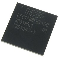
LPC1768FET100,551 NXP Semiconductors, LPC1768FET100,551 Datasheet - Page 16

LPC1768FET100,551
Manufacturer Part Number
LPC1768FET100,551
Description
IC MCU 32BIT 512KB FLASH 100LQFP
Manufacturer
NXP Semiconductors
Series
LPC17xxr
Datasheet
1.LPC1768FET100551.pdf
(79 pages)
Specifications of LPC1768FET100,551
Core Processor
ARM® Cortex-M3™
Core Size
32-Bit
Speed
100MHz
Connectivity
CAN, Ethernet, I²C, IrDA, Microwire, SPI, SSI, UART/USART, USB OTG
Peripherals
Brown-out Detect/Reset, DMA, I²S, Motor Control PWM, POR, PWM, WDT
Number Of I /o
70
Program Memory Size
512KB (512K x 8)
Program Memory Type
FLASH
Ram Size
64K x 8
Voltage - Supply (vcc/vdd)
2.4 V ~ 3.6 V
Data Converters
A/D 8x12b, D/A 1x10b
Oscillator Type
Internal
Operating Temperature
-40°C ~ 85°C
Package / Case
100-LQFP
Processor Series
LPC1768
Core
ARM Cortex-M3
Data Bus Width
32 bit
Data Ram Size
16 KB
Interface Type
Ethernet, USB, CAN, I2S, I2C
Maximum Clock Frequency
100 MHz
Number Of Programmable I/os
70
Number Of Timers
4
Maximum Operating Temperature
+ 150 C
Mounting Style
SMD/SMT
Lead Free Status / RoHS Status
Lead free / RoHS Compliant
Eeprom Size
-
Lead Free Status / Rohs Status
Details
Other names
568-5215
Available stocks
Company
Part Number
Manufacturer
Quantity
Price
Company:
Part Number:
LPC1768FET100,551
Manufacturer:
NXP Semiconductors
Quantity:
10 000
NXP Semiconductors
Table 4.
[1]
[2]
[3]
LPC1769_68_67_66_65_64_63
Product data sheet
Symbol
TDI
TMS/SWDIO
TRST
TCK/SWDCLK
RTCK
RSTOUT
RESET
XTAL1
XTAL2
RTCX1
RTCX2
V
V
V
V
V
VREFP
VREFN
VBAT
n.c.
SS
SSA
DD(3V3)
DD(REG)(3V3)
DDA
5 V tolerant pad providing digital I/O functions with TTL levels and hysteresis.
5 V tolerant pad providing digital I/O functions (with TTL levels and hysteresis) and analog input. When configured as a ADC input,
digital section of the pad is disabled and the pin is not 5 V tolerant.
5 V tolerant pad providing digital I/O with TTL levels and hysteresis and analog output function. When configured as the DAC output,
digital section of the pad is disabled.
Pin description
Pin
2
3
4
5
100
14
17
22
23
16
18
31, 41,
55, 72,
83, 97
11
28, 54,
71, 96
42, 84
10
12
15
19
13
[1][8]
[1][8]
[1][8]
[1][7]
[10]
[9]
[10][11]
[10][11]
[10][12]
[10]
[10]
[10]
[10][12]
[1][7]
[10]
[10]
[10]
…continued
Ball
C3
B1
C2
C1
B2
-
F3
H2
G3
F2
G1
B3, B7,
C9, G7,
J6, K3
E1
K2, H9,
C10,
A3
H6, A7
E2
E3
F1
G2
D4, E4
[9]
[10][11]
[1][8]
[1][7]
[10]
[10]
[10]
[10]
[1][8]
[1][8]
[1][7]
[10][11]
[10][11]
[10]
[10][12]
[10]
[10]
All information provided in this document is subject to legal disclaimers.
Type
I
I
I/O
I
I
I
O
O
I
I
O
I
O
I
I
I
I
I
I
I
I
-
Rev. 7 — 5 April 2011
Description
TDI — Test Data in for JTAG interface.
TMS — Test Mode Select for JTAG interface.
SWDIO — Serial wire debug data input/output.
TRST — Test Reset for JTAG interface.
TCK — Test Clock for JTAG interface.
SWDCLK — Serial wire clock.
RTCK — JTAG interface control signal.
RSTOUT — This is a 3.3 V pin. LOW on this pin indicates the
microcontroller being in Reset state.
External reset input: A LOW on this pin resets the device, causing I/O
ports and peripherals to take on their default states, and processor
execution to begin at address 0. TTL with hysteresis, 5 V tolerant.
Input to the oscillator circuit and internal clock generator circuits.
Output from the oscillator amplifier.
Input to the RTC oscillator circuit.
Output from the RTC oscillator circuit.
ground: 0 V reference.
analog ground: 0 V reference. This should nominally be the same
voltage as V
3.3 V supply voltage: This is the power supply voltage for the I/O
ports.
3.3 V voltage regulator supply voltage: This is the supply voltage for
the on-chip voltage regulator only.
analog 3.3 V pad supply voltage: This should be nominally the same
voltage as V
This voltage is used to power the ADC and DAC. This pin should be
tied to 3.3 V if the ADC and DAC are not used.
ADC positive reference voltage: This should be nominally the same
voltage as V
Level on this pin is used as a reference for ADC and DAC. This pin
should be tied to 3.3 V if the ADC and DAC are not used.
ADC negative reference voltage: This should be nominally the same
voltage as V
Level on this pin is used as a reference for ADC and DAC.
RTC pin power supply: 3.3 V on this pin supplies the power to the
RTC peripheral.
not connected.
LPC1769/68/67/66/65/64/63
SS
DD(3V3)
DDA
SS
, but should be isolated to minimize noise and error.
but should be isolated to minimize noise and error.
but should be isolated to minimize noise and error.
but should be isolated to minimize noise and error.
32-bit ARM Cortex-M3 microcontroller
© NXP B.V. 2011. All rights reserved.
16 of 79


