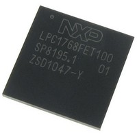
LPC1768FET100,551 NXP Semiconductors, LPC1768FET100,551 Datasheet - Page 19

LPC1768FET100,551
Manufacturer Part Number
LPC1768FET100,551
Description
IC MCU 32BIT 512KB FLASH 100LQFP
Manufacturer
NXP Semiconductors
Series
LPC17xxr
Datasheet
1.LPC1768FET100551.pdf
(79 pages)
Specifications of LPC1768FET100,551
Core Processor
ARM® Cortex-M3™
Core Size
32-Bit
Speed
100MHz
Connectivity
CAN, Ethernet, I²C, IrDA, Microwire, SPI, SSI, UART/USART, USB OTG
Peripherals
Brown-out Detect/Reset, DMA, I²S, Motor Control PWM, POR, PWM, WDT
Number Of I /o
70
Program Memory Size
512KB (512K x 8)
Program Memory Type
FLASH
Ram Size
64K x 8
Voltage - Supply (vcc/vdd)
2.4 V ~ 3.6 V
Data Converters
A/D 8x12b, D/A 1x10b
Oscillator Type
Internal
Operating Temperature
-40°C ~ 85°C
Package / Case
100-LQFP
Processor Series
LPC1768
Core
ARM Cortex-M3
Data Bus Width
32 bit
Data Ram Size
16 KB
Interface Type
Ethernet, USB, CAN, I2S, I2C
Maximum Clock Frequency
100 MHz
Number Of Programmable I/os
70
Number Of Timers
4
Maximum Operating Temperature
+ 150 C
Mounting Style
SMD/SMT
Lead Free Status / RoHS Status
Lead free / RoHS Compliant
Eeprom Size
-
Lead Free Status / Rohs Status
Details
Other names
568-5215
Available stocks
Company
Part Number
Manufacturer
Quantity
Price
Company:
Part Number:
LPC1768FET100,551
Manufacturer:
NXP Semiconductors
Quantity:
10 000
NXP Semiconductors
LPC1769_68_67_66_65_64_63
Product data sheet
7.6 Memory map
The MPU allows separating processing tasks by disallowing access to each other's data,
disabling access to memory regions, allowing memory regions to be defined as read-only
and detecting unexpected memory accesses that could potentially break the system.
The MPU separates the memory into distinct regions and implements protection by
preventing disallowed accesses. The MPU supports up to 8 regions each of which can be
divided into 8 subregions. Accesses to memory locations that are not defined in the MPU
regions, or not permitted by the region setting, will cause the Memory Management Fault
exception to take place.
The LPC17xx incorporates several distinct memory regions, shown in the following
figures.
program viewpoint following reset. The interrupt vector area supports address remapping.
The AHB peripheral area is 2 MB in size and is divided to allow for up to 128 peripherals.
The APB peripheral area is 1 MB in size and is divided to allow for up to 64 peripherals.
Each peripheral of either type is allocated 16 kB of space. This allows simplifying the
address decoding for each peripheral.
Figure 4
All information provided in this document is subject to legal disclaimers.
shows the overall map of the entire address space from the user
Rev. 7 — 5 April 2011
LPC1769/68/67/66/65/64/63
32-bit ARM Cortex-M3 microcontroller
© NXP B.V. 2011. All rights reserved.
19 of 79


