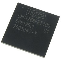
LPC1768FET100,551 NXP Semiconductors, LPC1768FET100,551 Datasheet - Page 22

LPC1768FET100,551
Manufacturer Part Number
LPC1768FET100,551
Description
IC MCU 32BIT 512KB FLASH 100LQFP
Manufacturer
NXP Semiconductors
Series
LPC17xxr
Datasheet
1.LPC1768FET100551.pdf
(79 pages)
Specifications of LPC1768FET100,551
Core Processor
ARM® Cortex-M3™
Core Size
32-Bit
Speed
100MHz
Connectivity
CAN, Ethernet, I²C, IrDA, Microwire, SPI, SSI, UART/USART, USB OTG
Peripherals
Brown-out Detect/Reset, DMA, I²S, Motor Control PWM, POR, PWM, WDT
Number Of I /o
70
Program Memory Size
512KB (512K x 8)
Program Memory Type
FLASH
Ram Size
64K x 8
Voltage - Supply (vcc/vdd)
2.4 V ~ 3.6 V
Data Converters
A/D 8x12b, D/A 1x10b
Oscillator Type
Internal
Operating Temperature
-40°C ~ 85°C
Package / Case
100-LQFP
Processor Series
LPC1768
Core
ARM Cortex-M3
Data Bus Width
32 bit
Data Ram Size
16 KB
Interface Type
Ethernet, USB, CAN, I2S, I2C
Maximum Clock Frequency
100 MHz
Number Of Programmable I/os
70
Number Of Timers
4
Maximum Operating Temperature
+ 150 C
Mounting Style
SMD/SMT
Lead Free Status / RoHS Status
Lead free / RoHS Compliant
Eeprom Size
-
Lead Free Status / Rohs Status
Details
Other names
568-5215
Available stocks
Company
Part Number
Manufacturer
Quantity
Price
Company:
Part Number:
LPC1768FET100,551
Manufacturer:
NXP Semiconductors
Quantity:
10 000
NXP Semiconductors
LPC1769_68_67_66_65_64_63
Product data sheet
7.9.1 Features
7.10 Fast general purpose parallel I/O
Device pins that are not connected to a specific peripheral function are controlled by the
GPIO registers. Pins may be dynamically configured as inputs or outputs. Separate
registers allow setting or clearing any number of outputs simultaneously. The value of the
output register may be read back as well as the current state of the port pins.
LPC17xx use accelerated GPIO functions:
•
•
•
•
•
•
•
•
•
•
•
•
•
•
•
•
•
•
•
•
•
•
Eight DMA channels. Each channel can support an unidirectional transfer.
16 DMA request lines.
Single DMA and burst DMA request signals. Each peripheral connected to the DMA
Controller can assert either a burst DMA request or a single DMA request. The DMA
burst size is set by programming the DMA Controller.
Memory-to-memory, memory-to-peripheral, peripheral-to-memory, and
peripheral-to-peripheral transfers are supported.
Scatter or gather DMA is supported through the use of linked lists. This means that
the source and destination areas do not have to occupy contiguous areas of memory.
Hardware DMA channel priority.
AHB slave DMA programming interface. The DMA Controller is programmed by
writing to the DMA control registers over the AHB slave interface.
One AHB bus master for transferring data. The interface transfers data when a DMA
request goes active.
32-bit AHB master bus width.
Incrementing or non-incrementing addressing for source and destination.
Programmable DMA burst size. The DMA burst size can be programmed to more
efficiently transfer data.
Internal four-word FIFO per channel.
Supports 8, 16, and 32-bit wide transactions.
Big-endian and little-endian support. The DMA Controller defaults to little-endian
mode on reset.
An interrupt to the processor can be generated on a DMA completion or when a DMA
error has occurred.
Raw interrupt status. The DMA error and DMA count raw interrupt status can be read
prior to masking.
GPIO registers are accessed through the AHB multilayer bus so that the fastest
possible I/O timing can be achieved.
Mask registers allow treating sets of port bits as a group, leaving other bits
unchanged.
All GPIO registers are byte and half-word addressable.
Entire port value can be written in one instruction.
Support for Cortex-M3 bit banding.
Support for use with the GPDMA controller.
All information provided in this document is subject to legal disclaimers.
Rev. 7 — 5 April 2011
LPC1769/68/67/66/65/64/63
32-bit ARM Cortex-M3 microcontroller
© NXP B.V. 2011. All rights reserved.
22 of 79


