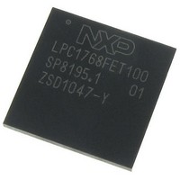
LPC1768FET100,551 NXP Semiconductors, LPC1768FET100,551 Datasheet - Page 28

LPC1768FET100,551
Manufacturer Part Number
LPC1768FET100,551
Description
IC MCU 32BIT 512KB FLASH 100LQFP
Manufacturer
NXP Semiconductors
Series
LPC17xxr
Datasheet
1.LPC1768FET100551.pdf
(79 pages)
Specifications of LPC1768FET100,551
Core Processor
ARM® Cortex-M3™
Core Size
32-Bit
Speed
100MHz
Connectivity
CAN, Ethernet, I²C, IrDA, Microwire, SPI, SSI, UART/USART, USB OTG
Peripherals
Brown-out Detect/Reset, DMA, I²S, Motor Control PWM, POR, PWM, WDT
Number Of I /o
70
Program Memory Size
512KB (512K x 8)
Program Memory Type
FLASH
Ram Size
64K x 8
Voltage - Supply (vcc/vdd)
2.4 V ~ 3.6 V
Data Converters
A/D 8x12b, D/A 1x10b
Oscillator Type
Internal
Operating Temperature
-40°C ~ 85°C
Package / Case
100-LQFP
Processor Series
LPC1768
Core
ARM Cortex-M3
Data Bus Width
32 bit
Data Ram Size
16 KB
Interface Type
Ethernet, USB, CAN, I2S, I2C
Maximum Clock Frequency
100 MHz
Number Of Programmable I/os
70
Number Of Timers
4
Maximum Operating Temperature
+ 150 C
Mounting Style
SMD/SMT
Lead Free Status / RoHS Status
Lead free / RoHS Compliant
Eeprom Size
-
Lead Free Status / Rohs Status
Details
Other names
568-5215
Available stocks
Company
Part Number
Manufacturer
Quantity
Price
Company:
Part Number:
LPC1768FET100,551
Manufacturer:
NXP Semiconductors
Quantity:
10 000
NXP Semiconductors
LPC1769_68_67_66_65_64_63
Product data sheet
7.18.1 Features
7.19.1 Features
7.19 I
data transfer. The SSP supports full duplex transfers, with frames of 4 bits to 16 bits of
data flowing from the master to the slave and from the slave to the master. In practice,
often only one of these data flows carries meaningful data.
The LPC17xx each contain three I
The I
(SCL) and a Serial DAta line (SDA). Each device is recognized by a unique address and
can operate as either a receiver-only device (e.g., an LCD driver) or a transmitter with the
capability to both receive and send information (such as memory). Transmitters and/or
receivers can operate in either master or slave mode, depending on whether the chip has
to initiate a data transfer or is only addressed. The I
controlled by more than one bus master connected to it.
2
•
•
•
•
•
•
•
•
•
•
•
•
•
•
•
•
•
•
C-bus serial I/O controllers
Maximum SSP speed of 50 Mbit/s (master) or 8 Mbit/s (slave)
Compatible with Motorola SPI, 4-wire Texas Instruments SSI, and National
Semiconductor Microwire buses
Synchronous serial communication
Master or slave operation
8-frame FIFOs for both transmit and receive
4-bit to 16-bit frame
DMA transfers supported by GPDMA
I
supports Fast mode plus with bit rates up to 1 Mbit/s.
I
Easy to configure as master, slave, or master/slave.
Programmable clocks allow versatile rate control.
Bidirectional data transfer between masters and slaves.
Multi-master bus (no central master).
Arbitration between simultaneously transmitting masters without corruption of serial
data on the bus.
Serial clock synchronization allows devices with different bit rates to communicate via
one serial bus.
Serial clock synchronization can be used as a handshake mechanism to suspend and
resume serial transfer.
The I
All I
2
2
2
C0 is a standard I
C1 and I
C-bus is bidirectional for inter-IC control using only two wires: a Serial Clock line
2
C-bus controllers support multiple address recognition and a bus monitor mode.
2
C-bus can be used for test and diagnostic purposes.
2
C2 use standard I/O pins with bit rates of up to 400 kbit/s (Fast I
All information provided in this document is subject to legal disclaimers.
2
C compliant bus interface with open-drain pins. I
Rev. 7 — 5 April 2011
LPC1769/68/67/66/65/64/63
2
C-bus controllers.
32-bit ARM Cortex-M3 microcontroller
2
C is a multi-master bus and can be
© NXP B.V. 2011. All rights reserved.
2
C0 also
2
C-bus).
28 of 79


