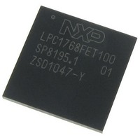
LPC1768FET100,551 NXP Semiconductors, LPC1768FET100,551 Datasheet - Page 9

LPC1768FET100,551
Manufacturer Part Number
LPC1768FET100,551
Description
IC MCU 32BIT 512KB FLASH 100LQFP
Manufacturer
NXP Semiconductors
Series
LPC17xxr
Datasheet
1.LPC1768FET100551.pdf
(79 pages)
Specifications of LPC1768FET100,551
Core Processor
ARM® Cortex-M3™
Core Size
32-Bit
Speed
100MHz
Connectivity
CAN, Ethernet, I²C, IrDA, Microwire, SPI, SSI, UART/USART, USB OTG
Peripherals
Brown-out Detect/Reset, DMA, I²S, Motor Control PWM, POR, PWM, WDT
Number Of I /o
70
Program Memory Size
512KB (512K x 8)
Program Memory Type
FLASH
Ram Size
64K x 8
Voltage - Supply (vcc/vdd)
2.4 V ~ 3.6 V
Data Converters
A/D 8x12b, D/A 1x10b
Oscillator Type
Internal
Operating Temperature
-40°C ~ 85°C
Package / Case
100-LQFP
Processor Series
LPC1768
Core
ARM Cortex-M3
Data Bus Width
32 bit
Data Ram Size
16 KB
Interface Type
Ethernet, USB, CAN, I2S, I2C
Maximum Clock Frequency
100 MHz
Number Of Programmable I/os
70
Number Of Timers
4
Maximum Operating Temperature
+ 150 C
Mounting Style
SMD/SMT
Lead Free Status / RoHS Status
Lead free / RoHS Compliant
Eeprom Size
-
Lead Free Status / Rohs Status
Details
Other names
568-5215
Available stocks
Company
Part Number
Manufacturer
Quantity
Price
Company:
Part Number:
LPC1768FET100,551
Manufacturer:
NXP Semiconductors
Quantity:
10 000
NXP Semiconductors
Table 4.
LPC1769_68_67_66_65_64_63
Product data sheet
Symbol
P0[4]/
I2SRX_CLK/
RD2/CAP2[0]
P0[5]/
I2SRX_WS/
TD2/CAP2[1]
P0[6]/
I2SRX_SDA/
SSEL1/MAT2[0]
P0[7]/
I2STX_CLK/
SCK1/MAT2[1]
P0[8]/
I2STX_WS/
MISO1/MAT2[2]
P0[9]/
I2STX_SDA/
MOSI1/MAT2[3]
P0[10]/TXD2/
SDA2/MAT3[0]
P0[11]/RXD2/
SCL2/MAT3[1]
Pin description
Pin
81
80
79
78
77
76
48
49
[1]
[1]
[1]
[1]
[1]
[1]
[1]
[1]
…continued
Ball
A8
D7
B8
A9
C8
A10
H7
K9
[1]
[1]
[1]
[1]
[1]
[1]
[1]
[1]
All information provided in this document is subject to legal disclaimers.
Type
I/O
I/O
I
I
I/O
I/O
O
I
I/O
I/O
I/O
O
I/O
I/O
I/O
O
I/O
I/O
I/O
O
I/O
I/O
I/O
O
I/O
O
I/O
O
I/O
I
I/O
O
Rev. 7 — 5 April 2011
Description
P0[4] — General purpose digital input/output pin.
I2SRX_CLK — Receive Clock. It is driven by the master and received
by the slave. Corresponds to the signal SCK in the I
specification. (LPC1769/68/67/66/65/63 only).
RD2 — CAN2 receiver input. (LPC1769/68/66/65/64 only).
CAP2[0] — Capture input for Timer 2, channel 0.
P0[5] — General purpose digital input/output pin.
I2SRX_WS — Receive Word Select. It is driven by the master and
received by the slave. Corresponds to the signal WS in the I
specification. (LPC1769/68/67/66/65/63 only).
TD2 — CAN2 transmitter output. (LPC1769/68/66/65/64 only).
CAP2[1] — Capture input for Timer 2, channel 1.
P0[6] — General purpose digital input/output pin.
I2SRX_SDA — Receive data. It is driven by the transmitter and read
by the receiver. Corresponds to the signal SD in the I
specification. (LPC1769/68/67/66/65/63 only).
SSEL1 — Slave Select for SSP1.
MAT2[0] — Match output for Timer 2, channel 0.
P0[7] — General purpose digital input/output pin.
I2STX_CLK — Transmit Clock. It is driven by the master and received
by the slave. Corresponds to the signal SCK in the I
specification. (LPC1769/68/67/66/65/63 only).
SCK1 — Serial Clock for SSP1.
MAT2[1] — Match output for Timer 2, channel 1.
P0[8] — General purpose digital input/output pin.
I2STX_WS — Transmit Word Select. It is driven by the master and
received by the slave. Corresponds to the signal WS in the I
specification. (LPC1769/68/67/66/65/63 only).
MISO1 — Master In Slave Out for SSP1.
MAT2[2] — Match output for Timer 2, channel 2.
P0[9] — General purpose digital input/output pin.
I2STX_SDA — Transmit data. It is driven by the transmitter and read
by the receiver. Corresponds to the signal SD in the I
specification. (LPC1769/68/67/66/65/63 only).
MOSI1 — Master Out Slave In for SSP1.
MAT2[3] — Match output for Timer 2, channel 3.
P0[10] — General purpose digital input/output pin.
TXD2 — Transmitter output for UART2.
SDA2 — I
MAT3[0] — Match output for Timer 3, channel 0.
P0[11] — General purpose digital input/output pin.
RXD2 — Receiver input for UART2.
SCL2 — I
MAT3[1] — Match output for Timer 3, channel 1.
LPC1769/68/67/66/65/64/63
2
2
C2 clock input/output (this is not an open-drain pin).
C2 data input/output (this is not an open-drain pin).
32-bit ARM Cortex-M3 microcontroller
© NXP B.V. 2011. All rights reserved.
2
2
S-bus
S-bus
2
2
S-bus
S-bus
2
2
S-bus
S-bus
9 of 79


