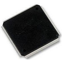
STM32F101ZGT6 STMicroelectronics, STM32F101ZGT6 Datasheet - Page 93

STM32F101ZGT6
Manufacturer Part Number
STM32F101ZGT6
Description
IC ARM CORTEX 1MB 144LQFP
Manufacturer
STMicroelectronics
Series
STM32r
Datasheet
1.STM32F101VGT6.pdf
(108 pages)
Specifications of STM32F101ZGT6
Core Processor
ARM® Cortex-M3™
Core Size
32-Bit
Speed
36MHz
Connectivity
I²C, IrDA, LIN, SPI, UART/USART
Peripherals
DMA, PDR, POR, PVD, PWM, Temp Sensor, WDT
Number Of I /o
112
Program Memory Size
1MB (1M x 8)
Program Memory Type
FLASH
Ram Size
80K x 8
Voltage - Supply (vcc/vdd)
2 V ~ 3.6 V
Data Converters
A/D 16x12b; D/A 2x12b
Oscillator Type
Internal
Operating Temperature
-40°C ~ 85°C
Package / Case
144-LFQFP
Processor Series
STM32F101xG
Core
ARM Cortex M3
Data Bus Width
32 bit
Data Ram Size
80 KB
Interface Type
I2C, SPI, UART
Maximum Clock Frequency
36 MHz
Number Of Programmable I/os
112
Number Of Timers
15
Operating Supply Voltage
2 V to 3.6 V
Maximum Operating Temperature
+ 85 C
Mounting Style
SMD/SMT
Operating Temperature Range
- 40 C to + 105 C
Processor To Be Evaluated
STM32F101ZG
Supply Current (max)
28 mA
Lead Free Status / RoHS Status
Lead free / RoHS Compliant
Eeprom Size
-
Lead Free Status / Rohs Status
Details
Available stocks
Company
Part Number
Manufacturer
Quantity
Price
Company:
Part Number:
STM32F101ZGT6
Manufacturer:
STMicroelectronics
Quantity:
135
Company:
Part Number:
STM32F101ZGT6
Manufacturer:
STMicroelectronics
Quantity:
40
Company:
Part Number:
STM32F101ZGT6
Manufacturer:
STMicroelectronics
Quantity:
10 000
STM32F101xF, STM32F101xG
Table 55.
1. Preliminary values.
2. Guaranteed by design, not tested in production.
3. V
4. For external triggers, a delay of 1/f
Equation 1: R
t
Symbol
t
R
C
STAB
f
R
CONV
t
V
TRIG
V
I
t
CAL
t
f
VREF
V
ADC
ADC
f
latr
t
R
AIN
lat
REF+
ADC
the package. Refer to
S
S
DDA
AIN
REF+
(2)
(2)
AIN
(2)
(2)
(2)
(2)
(2)
(2)
(2)
(2)
(2)
can be internally connected to V
------------------------------------------------------------- - R
f
Power supply
Positive reference voltage
Current on the V
pin
ADC clock frequency
Sampling rate
External trigger frequency
Conversion voltage range
External input impedance
Sampling switch resistance
Internal sample and hold
capacitor
Calibration time
Injection trigger conversion
latency
Regular trigger conversion
latency
Sampling time
Power-up time
Total conversion time
(including sampling time)
ADC
ADC characteristics
AIN
C
Parameter
ADC
max formula:
T
Section 3: Pinouts and pin descriptions
S
ln
REF
2
N
input
+
Doc ID 17143 Rev 2
PCLK2
2
(3)
–
DDA
must be added to the latency specified in
f
1
f
f
f
f
f
ADC
See
ADC
ADC
ADC
ADC
ADC
ADC
and V
and
Conditions
for details
= 14 MHz
= 14 MHz
= 14 MHz
= 14 MHz
= 14 MHz
= 14 MHz
Equation
Table 56
REF-
can be internally connected to V
14 to 252 (t
successive approximation)
0 (V
tied to ground)
for further details.
SSA
0.107
0.05
Min
2.4
2.4
0.6
1.5
0
1
or V
S
REF-
for sampling +12.5 for
Electrical characteristics
5.9
83
160
Table
Typ
0
(1)
SSA
55.
, depending on
V
220
0.214
0.143
239.5
V
Max
17.1
823
3
2
3.6
REF+
14
17
50
18
DDA
1
1
8
1
(4)
(4)
(1)
1/f
1/f
1/f
1/f
1/f
1/f
93/108
MHz
MHz
Unit
kHz
µA
k
k
pF
µs
µs
µs
µs
µs
µs
V
V
V
ADC
ADC
ADC
ADC
ADC
ADC


