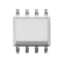
FAN3214TMX Fairchild Semiconductor, FAN3214TMX Datasheet

FAN3214TMX
Specifications of FAN3214TMX
Available stocks
Related parts for FAN3214TMX
FAN3214TMX Summary of contents
Page 1
... Synchronous Rectifier Circuits DC-to-DC Converters Motor Control Ordering Information Part Number FAN3213TMX Dual Inverting Channels FAN3214TMX Dual Non-Inverting Channels © 2008 Fairchild Semiconductor Corporation FAN3213 / FAN3214 • Rev. 1.0.2 Description The FAN3213 and FAN3214 dual 4A gate drivers are designed = 12V MOSFETs ...
Page 2
... Psi_JT ( ): Thermal characterization parameter providing correlation between the semiconductor junction temperature and JT the center of the top of the package for the thermal environment defined in Note 4. © 2008 Fairchild Semiconductor Corporation FAN3213 / FAN3214 • Rev. 1.0.2 Figure 2. SOIC-8 (Top View) (1) (2) JL ...
Page 3
... No Connect. This pin can be grounded or left floating. Output Logic FAN3213 (x INx 0 ( (7) 1 Note: 7. Default input signal if no external connection is made. © 2008 Fairchild Semiconductor Corporation FAN3213 / FAN3214 • Rev. 1.0.2 FAN3213 Figure 3. Pin Configurations (Repeated) Pin Description is above UVLO threshold above UVLO threshold. DD FAN3214 (x INx OUTx (7) ...
Page 4
... Block Diagrams © 2008 Fairchild Semiconductor Corporation FAN3213 / FAN3214 • Rev. 1.0.2 Figure 4. FAN3213 Block Diagram Figure 5. FAN3214 Block Diagram 4 www.fairchildsemi.com ...
Page 5
... Supply Voltage Range DD V Input Voltage INA, INA+, INA–, INB, INB+ and INB– Operating Ambient Temperature A © 2008 Fairchild Semiconductor Corporation FAN3213 / FAN3214 • Rev. 1.0.2 Parameter Human Body Model, JEDEC JESD22-A114 Charged Device Model, JEDEC JESD22-C101 Parameter 5 Min. ...
Page 6
... RVS Notes: 8. Not tested in production. 9. See Timing Diagrams of Figure 6 and Figure 7. Figure 6. Non-Inverting Timing Diagram © 2008 Fairchild Semiconductor Corporation FAN3213 / FAN3214 • Rev. 1.0.2 =-40°C to +125°C. Currents are defined as positive into the device and negative J Conditions INA = V , INB = 0V DD ...
Page 7
... Typical Performance Characteristics Typical characteristics are provided at T Figure 8. I (Static) vs. Supply Voltage DD Figure 10. I (No Load) vs. Frequency DD Figure 12. Input Thresholds vs. Supply Voltage © 2008 Fairchild Semiconductor Corporation FAN3213 / FAN3214 • Rev. 1.0.2 =25°C and V =12V unless otherwise noted (10) Figure 9. I Figure 11. I Figure 13 ...
Page 8
... Typical Performance Characteristics Typical characteristics are provided at T Figure 14. Propagation Delay vs. Supply Voltage Figure 16. Propagation Delays vs. Temperature © 2008 Fairchild Semiconductor Corporation FAN3213 / FAN3214 • Rev. 1.0.2 =25°C and V =12V unless otherwise noted UVLO Threshold vs. Temperature Figure 15. Propagation Delay vs. Supply Voltage Figure 17 ...
Page 9
... Typical Performance Characteristics Typical characteristics are provided at T Figure 18. Fall Time vs. Supply Voltage Figure 21. Rise/Fall Waveforms with 2.2nF Load © 2008 Fairchild Semiconductor Corporation FAN3213 / FAN3214 • Rev. 1.0.2 =25°C and V =12V unless otherwise noted Figure 19. Rise Time vs. Supply Voltage Figure 20. Rise and Fall Times vs. Temperature Figure 22 ...
Page 10
... Figure 4 and Figure 5. 11. The initial spike in each current waveform is a measurement artifact caused by the stray inductance of the current- measurement loop. Test Circuit © 2008 Fairchild Semiconductor Corporation FAN3213 / FAN3214 • Rev. 1.0.2 =25°C and V =12V unless otherwise noted. ...
Page 11
... The output pin slew rate is determined by V and the load on the output not user adjustable, but a series resistor can be added if a slower rise or fall time at the MOSFET gate is needed. © 2008 Fairchild Semiconductor Corporation FAN3213 / FAN3214 • Rev. 1.0.2 voltage, and there is DD Figure 28. MillerDrive™ ...
Page 12
... MOSFET circuit, preventing them from disturbing the sensitive analog circuitry in the PWM controller. © 2008 Fairchild Semiconductor Corporation FAN3213 / FAN3214 • Rev. 1.0.2 Figure 29. Current Path for MOSFET Turn-On Figure 30 shows the current path when the gate driver turns the MOSFET OFF ...
Page 13
... LOW until the UVLO threshold is reached, then the output is in-phase with the input. Figure 31. Non-Inverting Startup Waveforms © 2008 Fairchild Semiconductor Corporation FAN3213 / FAN3214 • Rev. 1.0.2 The inverting configuration of startup waveforms are shown in Figure 32. With IN+ tied to VDD and the input until steady- signal applied to IN– ...
Page 14
... T = board temperature in location as defined in B the Thermal Characteristics table. © 2008 Fairchild Semiconductor Corporation FAN3213 / FAN3214 • Rev. 1.0.2 To give a numerical example, if the synchronous rectifier switches in the forward converter of Figure 33 are FDMS8660S, the datasheet gives a total gate charge of 60nC 120nC gate charge ...
Page 15
... Typical Application Diagrams Figure 33. High-Current Forward Converter with Synchronous Rectification Vin FAN3227 Figure 35. Secondary Controlled Full Bridge with Current Doubler Output, © 2008 Fairchild Semiconductor Corporation FAN3213 / FAN3214 • Rev. 1.0.2 Figure 34 PWM-A FAN3227 Secondary PWM-B Phase Shift Controller PWM-C PWM-D ...
Page 16
... Single 9A FAN3122T +9.7A / -7.1A Single 9A FAN3122C +9.7A / -7.1A Notes: 12. Typical currents with OUTx at 6V and V 13. Thresholds proportional to an externally supplied reference voltage. © 2008 Fairchild Semiconductor Corporation FAN3213 / FAN3214 • Rev. 1.0.2 (12) Input Threshold CMOS Single Channel of Dual-Input/Single-Output (13) External Single Non-Inverting Channel with External Reference SOT23-5, MLP6 ...
Page 17
... Package drawings are provided as a service to customers considering Fairchild components. Drawings may change in any manner without notice. Please note the revision and/or date on the drawing and contact a Fairchild Semiconductor representative to verify or obtain the most recent revision. Package specifications do not expand the terms of Fairchild’s worldwide terms and conditions, specifically the warranty therein, which covers Fairchild products. Always visit Fairchild Semiconductor’ ...
Page 18
... Fairchild Semiconductor Corporation FAN3213 / FAN3214 • Rev. 1.0.2 18 www.fairchildsemi.com ...


