74LVC2T45GD,125 NXP Semiconductors, 74LVC2T45GD,125 Datasheet - Page 3
74LVC2T45GD,125
Manufacturer Part Number
74LVC2T45GD,125
Description
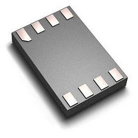
TXRX TRANSLATING 3ST XSON8U
Manufacturer
NXP Semiconductors
Datasheet
1.74LVC2T45GD125.pdf
(36 pages)
Specifications of 74LVC2T45GD,125
Logic Family
74LVC
Number Of Channels Per Chip
2
Propagation Delay Time
15.2 ns
Supply Voltage (max)
5.5 V
Supply Voltage (min)
1.2 V
Maximum Operating Temperature
+ 125 C
Package / Case
XSON-8U
Maximum Power Dissipation
250 mW
Minimum Operating Temperature
- 40 C
Mounting Style
SMD/SMT
Lead Free Status / RoHS Status
Lead free / RoHS Compliant
Other names
568-5480-2


NXP Semiconductors
Table 2.
[1]
5. Functional diagram
6. Pinning information
74LVC_LVCH2T45
Product data sheet
Type number
74LVC2T45GN
74LVCH2T45GN
74LVC2T45GS
74LVCH2T45GS
Fig 1.
Fig 3.
The pin 1 indicator is located on the lower left corner of the device, below the marking code.
DIR
Logic symbol
1A
2A
Pin configuration SOT765-1
Marking
V
CC(A)
GND
5
2
3
1A
2A
6.1 Pinning
1
2
3
4
…continued
V
CC(A)
74LVCH2T45
74LVC2T45
001aai904
V
CC(B)
001aag577
8
7
6
5
All information provided in this document is subject to legal disclaimers.
V
1B
2B
DIR
CC(B)
7
6
1B
2B
Rev. 4 — 20 August 2010
Marking code
V5
X5
V5
X5
Fig 2.
Fig 4.
74LVC2T45; 74LVCH2T45
Logic diagram
Pin configuration SOT833-1, SOT1089,
SOT1116 and SOT1203
Dual supply translating transceiver; 3-state
DIR
1A
2A
[1]
V
CC(A)
GND
1A
2A
V
CC(A)
Transparent top view
74LVCH2T45
74LVC2T45
1
2
3
4
001aai905
8
7
6
5
V
CC(B)
001aag578
V
1B
2B
DIR
CC(B)
© NXP B.V. 2010. All rights reserved.
1B
2B
3 of 36
Related parts for 74LVC2T45GD,125
Image
Part Number
Description
Manufacturer
Datasheet
Request
R

Part Number:
Description:
Dual Supply Translating Transceiver; 3-state
Manufacturer:
NXP Semiconductors
Datasheet:
Part Number:
Description:
NXP Semiconductors designed the LPC2420/2460 microcontroller around a 16-bit/32-bitARM7TDMI-S CPU core with real-time debug interfaces that include both JTAG andembedded trace
Manufacturer:
NXP Semiconductors
Datasheet:

Part Number:
Description:
NXP Semiconductors designed the LPC2458 microcontroller around a 16-bit/32-bitARM7TDMI-S CPU core with real-time debug interfaces that include both JTAG andembedded trace
Manufacturer:
NXP Semiconductors
Datasheet:
Part Number:
Description:
NXP Semiconductors designed the LPC2468 microcontroller around a 16-bit/32-bitARM7TDMI-S CPU core with real-time debug interfaces that include both JTAG andembedded trace
Manufacturer:
NXP Semiconductors
Datasheet:
Part Number:
Description:
NXP Semiconductors designed the LPC2470 microcontroller, powered by theARM7TDMI-S core, to be a highly integrated microcontroller for a wide range ofapplications that require advanced communications and high quality graphic displays
Manufacturer:
NXP Semiconductors
Datasheet:
Part Number:
Description:
NXP Semiconductors designed the LPC2478 microcontroller, powered by theARM7TDMI-S core, to be a highly integrated microcontroller for a wide range ofapplications that require advanced communications and high quality graphic displays
Manufacturer:
NXP Semiconductors
Datasheet:
Part Number:
Description:
The Philips Semiconductors XA (eXtended Architecture) family of 16-bit single-chip microcontrollers is powerful enough to easily handle the requirements of high performance embedded applications, yet inexpensive enough to compete in the market for hi
Manufacturer:
NXP Semiconductors
Datasheet:
Part Number:
Description:
The XA-S3 device is a member of Philips Semiconductors? XA(eXtended Architecture) family of high performance 16-bitsingle-chip microcontrollers
Manufacturer:
NXP Semiconductors
Datasheet:

Part Number:
Description:
The NXP BlueStreak LH75401/LH75411 family consists of two low-cost 16/32-bit System-on-Chip (SoC) devices
Manufacturer:
NXP Semiconductors
Datasheet:
Part Number:
Description:
The NXP LPC3130/3131 combine an 180 MHz ARM926EJ-S CPU core, high-speed USB2
Manufacturer:
NXP Semiconductors
Datasheet:
Part Number:
Description:
The NXP LPC3141 combine a 270 MHz ARM926EJ-S CPU core, High-speed USB 2
Manufacturer:
NXP Semiconductors
Part Number:
Description:
The NXP LPC3143 combine a 270 MHz ARM926EJ-S CPU core, High-speed USB 2
Manufacturer:
NXP Semiconductors

Part Number:
Description:
The NXP LPC3152 combines an 180 MHz ARM926EJ-S CPU core, High-speed USB 2
Manufacturer:
NXP Semiconductors
Part Number:
Description:
The NXP LPC3154 combines an 180 MHz ARM926EJ-S CPU core, High-speed USB 2
Manufacturer:
NXP Semiconductors