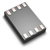
74LVC2T45GT,115 NXP Semiconductors, 74LVC2T45GT,115 Datasheet - Page 11

74LVC2T45GT,115
Manufacturer Part Number
74LVC2T45GT,115
Description
TXRX TRANSLATING 3ST XSON8
Manufacturer
NXP Semiconductors
Datasheet
1.74LVC2T45GD125.pdf
(36 pages)
Specifications of 74LVC2T45GT,115
Logic Family
74LVC
Number Of Channels Per Chip
2
Propagation Delay Time
15.2 ns
Supply Voltage (max)
5.5 V
Supply Voltage (min)
1.2 V
Maximum Operating Temperature
+ 125 C
Package / Case
XSON-8
Maximum Power Dissipation
250 mW
Minimum Operating Temperature
- 40 C
Mounting Style
SMD/SMT
Lead Free Status / RoHS Status
Lead free / RoHS Compliant
Other names
568-5482-2
NXP Semiconductors
Table 11.
Voltages are referenced to GND (ground = 0 V).
[1]
[2]
Table 12.
Voltages are referenced to GND (ground = 0 V); for test circuit see
74LVC_LVCH2T45
Product data sheet
Symbol Parameter
C
Symbol Parameter
V
t
t
t
t
t
t
V
t
t
t
t
PLH
PHL
PHZ
PLZ
PZH
PZL
PLH
PHL
PHZ
PLZ
CC(A)
CC(A)
PD
C
P
f
f
C
V
N = number of inputs switching;
Σ(C
f
i
o
i
D
CC
PD
= input frequency in MHz;
L
= 10 MHz; V
= output frequency in MHz;
= load capacitance in pF;
= C
= 1.4 V to 1.6 V
= 1.65 V to 1.95 V
L
is used to determine the dynamic power dissipation (P
= supply voltage in V;
× V
LOW to HIGH
propagation delay
HIGH to LOW
propagation delay
HIGH to OFF-state
propagation delay
LOW to OFF-state
propagation delay
OFF-state to HIGH
propagation delay
OFF-state to LOW
propagation delay
LOW to HIGH
propagation delay
HIGH to LOW
propagation delay
HIGH to OFF-state
propagation delay
LOW to OFF-state
propagation delay
power dissipation
capacitance
PD
Typical power dissipation capacitance at V
Dynamic characteristics for temperature range −40 °C to +85 °C
CC
× V
2
× f
CC
I
o
= GND to V
2
) = sum of the outputs.
× f
i
× N + Σ(C
CC
; t
Conditions
A port: (direction A to B);
B port: (direction B to A)
A port: (direction B to A);
B port: (direction A to B)
Conditions
A to B
B to A
A to B
B to A
DIR to A
DIR to B
DIR to A
DIR to B
DIR to A
DIR to B
DIR to A
DIR to B
A to B
B to A
A to B
B to A
DIR to A
DIR to B
DIR to A
DIR to B
L
r
× V
= t
f
CC
= 1 ns; C
2
× f
o
[1]
[1]
[1]
[1]
All information provided in this document is subject to legal disclaimers.
) where:
L
1.5 V ± 0.1 V 1.8 V ± 0.15 V 2.5 V ± 0.2 V 3.3 V ± 0.3 V 5.0 V ± 0.5 V
= 0 pF; R
Min
2.8
2.8
2.6
2.6
3.0
3.5
2.4
2.8
2.6
2.4
2.4
2.2
2.9
3.2
2.4
2.5
-
-
-
-
Rev. 4 — 20 August 2010
Max
21.3
21.3
19.3
19.3
18.7
24.8
18.3
39.6
32.7
44.1
38.0
19.1
17.6
17.3
15.3
17.1
24.1
10.5
17.6
11.4
L
= ∞ Ω.
D
CC(A)
in μW).
Min
3.0
3.5
2.9
3.2
2.4
2.4
2.6
2.2
2.4
2.4
3.0
2.2
2.2
2.0
2.0
2.6
-
-
-
-
= V
74LVC2T45; 74LVCH2T45
1.8 V
CC(B)
Figure
15
2
Max
17.6
19.1
15.3
17.3
18.7
23.6
17.2
36.3
29.0
40.9
34.0
17.7
17.7
14.3
14.3
17.1
21.9
10.5
16.0
11.4
and T
Dual supply translating transceiver; 3-state
9; for wave forms see
Min
3.0
3.0
2.9
2.7
2.4
2.0
2.3
1.8
2.3
2.4
2.5
2.2
2.3
1.6
2.1
2.2
amb
-
-
-
-
V
CC(B)
2.5 V
V
16
= 25 °C
3
CC(A)
Max
13.5
14.9
13.2
18.7
24.3
24.9
24.2
30.5
16.0
12.9
17.1
10.5
11.8
11.0
11.4
11.5
9.4
9.3
8.5
9.2
and V
[1][2]
Min
1.7
2.3
1.7
2.2
3.0
3.3
2.4
3.0
1.7
2.1
1.8
2.0
2.9
3.0
2.4
2.7
-
-
-
-
CC(B)
3.3 V
16
Figure 7
3
18.7
22.5
23.2
22.6
29.6
17.1
10.3
10.5
Max
11.8
12.4
10.9
11.3
11.3
11.4
10.1
15.5
12.6
7.2
7.1
8.4
© NXP B.V. 2010. All rights reserved.
and
Min
1.6
2.2
1.7
2.3
3.0
2.8
2.4
2.5
1.4
1.9
1.7
1.8
2.9
2.5
2.4
2.4
-
-
-
-
5.0 V
Figure
18
4
Max
10.5 ns
12.0 ns
10.8 ns
18.7 ns
10.3 ns
21.4 ns
21.9 ns
21.3 ns
29.5 ns
15.1 ns
12.2 ns
17.1 ns
10.5 ns
11.0 ns
11.4 ns
9.4
6.8
7.0
8.2
7.1
8.
11 of 36
Unit
pF
pF
Unit
ns
ns
ns
ns
ns


