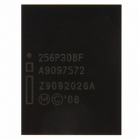
RC28F256P30BFA NUMONYX, RC28F256P30BFA Datasheet - Page 22

RC28F256P30BFA
Manufacturer Part Number
RC28F256P30BFA
Description
IC FLASH 256MBIT 100NS 64EZBGA
Manufacturer
NUMONYX
Series
Axcell™r
Datasheet
1.PF48F4000P0ZBQEF.pdf
(94 pages)
Specifications of RC28F256P30BFA
Format - Memory
FLASH
Memory Type
FLASH
Memory Size
256M (16Mx16)
Speed
100ns
Interface
Parallel
Voltage - Supply
1.7 V ~ 2 V
Operating Temperature
-40°C ~ 85°C
Package / Case
64-EZBGA
Lead Free Status / RoHS Status
Contains lead / RoHS non-compliant
Other names
898885
898885
RC28F256P30BF 898885
898885
RC28F256P30BF 898885
Available stocks
Company
Part Number
Manufacturer
Quantity
Price
Company:
Part Number:
RC28F256P30BFA
Manufacturer:
MICRON
Quantity:
1 000
Company:
Part Number:
RC28F256P30BFA
Manufacturer:
Micron Technology Inc
Quantity:
10 000
Table 8:
Datasheet
22
Block Locking/
Configuration
Blank Check
Protection
Unlocking
Suspend
Mode
EFI
(1)
Command Codes and Definitions (Sheet 2 of 2)
Code
0xD0
0xD0
0xD0
0xBC
0xD0
0xB0
0x60
0x01
0x2F
0x60
0x01
0x2F
0xC0
0x60
0x03
0xEB
Program or Erase
Suspend
Suspend Resume
Block lock Setup
Block lock
Block Unlock
Block Lock-Down
Block lock Setup
Block lock
Block Unlock
Block Lock-Down
OTP Register or
Lock Register
program setup
Read Configuration
Register Setup
Read Configuration
Register
Block Blank Check
Block Blank Check
Confirm
Extended Function
Interface command
Device Mode
This command issued to any device address initiates a suspend of the
currently-executing program or block erase operation. The Status Register
indicates successful suspend operation by setting either SR.2 (program
suspended) or SR.6 (erase suspended), along with SR.7 (ready). The Write
State Machine remains in the suspend mode regardless of control signal
states (except for RST# asserted).
This command issued to any device address resumes the suspended program
or block-erase operation.
First cycle of a 2-cycle command; prepares the CUI for block lock
configuration changes. If the next command is not Block Lock (0x01), Block
Unlock (0xD0), or Block Lock-Down (0x2F), the CUI sets Status Register bits
SR.5 and SR.4, indicating a command sequence error.
If the previous command was Block Lock Setup (0x60), the addressed block
is locked.
If the previous command was Block Lock Setup (0x60), the addressed block
is unlocked. If the addressed block is in a lock-down state, the operation has
no effect.
If the previous command was Block Lock Setup (0x60), the addressed block
is locked down.
First cycle of a 2-cycle command; prepares the device for a OTP register or
Lock Register program operation. The second cycle latches the register
address and data, and starts the programming algorithm to program data the
the OTP array.
First cycle of a 2-cycle command; prepares the CUI for device read
configuration. If the Set Read Configuration Register command (0x03) is not
the next command, the CUI sets Status Register bits SR.4 and SR.5,
indicating a command sequence error.
If the previous command was Read Configuration Register Setup (0x60), the
CUI latches the address and writes A[16:1] to the Read Configuration
Register for Easy BGA and TSOP, A[15:0] for QUAD+. Following a Configure
Read Configuration Register command, subsequent read operations access
array data.
First cycle of a 2-cycle command; initiates the Blank Check operation on a
main block.
Second cycle of blank check command sequence; it latches the block address
and executes blank check on the main array block.
First cycle of a multiple-cycle command; initiate operation using extended
function interface. The second cycle is a Sub-Op-Code, the data written on
third cycle is one less than the word count; the allowable value on this cycle
are 0 through 511. The subsequent cycles load data words into the program
buffer at a specified address until word count is achieved.
Description
Order Number: 320002-10
P30-65nm
Mar 2010


