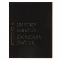
RC28F256P30BFA NUMONYX, RC28F256P30BFA Datasheet - Page 33

RC28F256P30BFA
Manufacturer Part Number
RC28F256P30BFA
Description
IC FLASH 256MBIT 100NS 64EZBGA
Manufacturer
NUMONYX
Series
Axcell™r
Datasheet
1.PF48F4000P0ZBQEF.pdf
(94 pages)
Specifications of RC28F256P30BFA
Format - Memory
FLASH
Memory Type
FLASH
Memory Size
256M (16Mx16)
Speed
100ns
Interface
Parallel
Voltage - Supply
1.7 V ~ 2 V
Operating Temperature
-40°C ~ 85°C
Package / Case
64-EZBGA
Lead Free Status / RoHS Status
Contains lead / RoHS non-compliant
Other names
898885
898885
RC28F256P30BF 898885
898885
RC28F256P30BF 898885
Available stocks
Company
Part Number
Manufacturer
Quantity
Price
Company:
Part Number:
RC28F256P30BFA
Manufacturer:
MICRON
Quantity:
1 000
Company:
Part Number:
RC28F256P30BFA
Manufacturer:
Micron Technology Inc
Quantity:
10 000
P30-65nm
9.0
9.1
9.2
Datasheet
33
Erase Operations
Flash erasing is performed on a block basis. An entire block is erased each time an
erase command sequence is issued, and only one block is erased at a time. When a
block is erased, all bits within that block read as logical ones. The following sections
describe block erase operations in detail.
Block Erase
Block erase operations are initiated by writing the Block Erase Setup command to the
address of the block to be erased (see
the Block Erase Confirm command is written to the address of the block to be erased. If
the device is placed in standby (CE# deasserted) during an erase operation, the device
completes the erase operation before entering standby.V
the block must be unlocked (see
During a block erase, the Write State Machine (WSM) executes a sequence of
internally-timed events that conditions, erases, and verifies all bits within the block.
Erasing the flash memory array changes “zeros” to “ones”. Memory block array that are
ones can be changed to zeros only by programming the block (see
“Program Operation” on page
The Status Register can be examined for block erase progress and errors by reading
any address. The device remains in the Read Status Register state until another
command is written. SR.0 indicates whether the addressed block is erasing. Status
Register bit SR.7 is set upon erase completion.
Status Register bit SR.7 indicates block erase status while the sequence executes.
When the erase operation has finished, Status Register bit SR.5 indicates an erase
failure if set. SR.3 set would indicate that the WSM could not perform the erase
operation because V
erase operation attempted to erase a locked block, causing the operation to abort.
Before issuing a new command, the Status Register contents should be examined and
then cleared using the Clear Status Register command. Any valid command can follow
once the block erase operation has completed.
Blank Check
The Blank Check operation determines whether a specified main block is blank (i.e.
completely erased). Without Blank Check, Block Erase would be the only other way to
ensure a block is completely erased. Blank Check is especially useful in the case of
erase operation interrupted by a power loss event.
Blank check can apply to only one block at a time, and no operations other than Status
Register Reads are allowed during Blank Check (e.g. reading array data, program,
erase etc). Suspend and resume operations are not supported during Blank Check, nor
is Blank Check supported during any suspended operations.
Blank Check operations are initiated by writing the Blank Check Setup command to the
block address. Next, the Check Confirm command is issued along with the same block
address. When a successful command sequence is entered, the device automatically
enters the Read Status State. The WSM then reads the entire specified block, and
determines whether any bit in the block is programmed or over-erased.
PP
was outside of its acceptable limits. SR.1 set indicates that the
27).
Figure 39, “Block Erase Flowchart” on page
Section 6.0, “Command Set” on page
PP
must be above V
Order Number: 320002-10
Section 8.0,
PPLK
21). Next,
82).
Mar 2010
and


