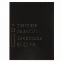
RC28F256P30BFA NUMONYX, RC28F256P30BFA Datasheet - Page 40

RC28F256P30BFA
Manufacturer Part Number
RC28F256P30BFA
Description
IC FLASH 256MBIT 100NS 64EZBGA
Manufacturer
NUMONYX
Series
Axcell™r
Datasheet
1.PF48F4000P0ZBQEF.pdf
(94 pages)
Specifications of RC28F256P30BFA
Format - Memory
FLASH
Memory Type
FLASH
Memory Size
256M (16Mx16)
Speed
100ns
Interface
Parallel
Voltage - Supply
1.7 V ~ 2 V
Operating Temperature
-40°C ~ 85°C
Package / Case
64-EZBGA
Lead Free Status / RoHS Status
Contains lead / RoHS non-compliant
Other names
898885
898885
RC28F256P30BF 898885
898885
RC28F256P30BF 898885
Available stocks
Company
Part Number
Manufacturer
Quantity
Price
Company:
Part Number:
RC28F256P30BFA
Manufacturer:
MICRON
Quantity:
1 000
Company:
Part Number:
RC28F256P30BFA
Manufacturer:
Micron Technology Inc
Quantity:
10 000
Table 15: Read Configuration Register Description (Sheet 2 of 2)
11.2.1
11.2.2
Datasheet
40
14:11
10
9
8
7
6
5:4
3
2:0
Latency Count (LC[3:0])
WAIT Polarity (WP)
Reserved (R)
WAIT Delay (WD)
Burst Sequence (BS)
Clock Edge (CE)
Reserved (R)
Burst Wrap (BW)
Burst Length (BL[2:0])
Read Mode
The Read Mode (RM) bit selects synchronous burst-mode or asynchronous page-mode
operation for the device. When the RM bit is set, asynchronous page mode is selected
(default). When RM is cleared, synchronous burst mode is selected.
Latency Count
The Latency Count (LC) bits tell the device how many clock cycles must elapse from the
rising edge of ADV# (or from the first valid clock edge after ADV# is asserted) until the
first valid data word is to be driven onto DQ[15:0]. The input clock frequency is used to
determine this value and
settings of LC. The minimum Latency Count for P30-65nm would be Code 4 based on
the Max Clock frequency specification of 52 MHz, and there will be zero WAIT States
when bursting within the word line. Please also refer to
Line (EOWL) Considerations” on page 42
Refer to
Table 16, “LC and Frequency Support” on page 42
0010 =Code 2
0011 =Code 3
0100 =Code 4
0101 =Code 5
0110 =Code 6
0111 =Code 7
1000 =Code 8
1001 =Code 9
1010 =Code 10
1011 =Code 11
1100 =Code 12
1101 =Code 13
1110 =Code 14
1111 =Code 15 (default)
(Other bit settings are reserved)
0 =WAIT signal is active low (default)
1 =WAIT signal is active high
Default “0”, Non-changeable
0 =WAIT deasserted with valid data
1 =WAIT deasserted one data cycle before valid data (default)
Default “0”, Non-changeable
0 = Falling edge
1 = Rising edge (default)
Default “0”, Non-changeable
0 =Wrap; Burst accesses wrap within burst length set by BL[2:0]
1 =No Wrap; Burst accesses do not wrap within burst length (default)
001 =4-word burst
010 =8-word burst
011 =16-word burst
111 =Continuous-word burst (default)
(Other bit settings are reserved)
Figure 13
shows the data output latency for the different
for more information on EOWL.
Section 11.2.3, “End of Word
for Latency Code Settings.
Order Number: 320002-10
P30-65nm
Mar 2010


