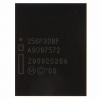
RC28F256P30BFA NUMONYX, RC28F256P30BFA Datasheet - Page 93

RC28F256P30BFA
Manufacturer Part Number
RC28F256P30BFA
Description
IC FLASH 256MBIT 100NS 64EZBGA
Manufacturer
NUMONYX
Series
Axcell™r
Datasheet
1.PF48F4000P0ZBQEF.pdf
(94 pages)
Specifications of RC28F256P30BFA
Format - Memory
FLASH
Memory Type
FLASH
Memory Size
256M (16Mx16)
Speed
100ns
Interface
Parallel
Voltage - Supply
1.7 V ~ 2 V
Operating Temperature
-40°C ~ 85°C
Package / Case
64-EZBGA
Lead Free Status / RoHS Status
Contains lead / RoHS non-compliant
Other names
898885
898885
RC28F256P30BF 898885
898885
RC28F256P30BF 898885
Available stocks
Company
Part Number
Manufacturer
Quantity
Price
Company:
Part Number:
RC28F256P30BFA
Manufacturer:
MICRON
Quantity:
1 000
Company:
Part Number:
RC28F256P30BFA
Manufacturer:
Micron Technology Inc
Quantity:
10 000
P30-65nm
Appendix C Revision History
Datasheet
93
Revision Date
Mar 2010
Aug 2009
Dec 2008
Nov 2008
Nov 2008
Sep 2008
July 2008
Apr 2009
Jan 2008
Revision
10
09
08
07
06
05
04
03
02
Program performance update in front page,
Specifications”
t
page 59
Erase/program suspend latency specification update,
Erase Specifications” on page 63
Leaded TSOP part EOL.
Burst latency update and 40MHz spec update,
Support” on page 42
Clarify the capacitance,
Ordering Information update.
QUAD+ ball height correction to 0.2mm in
Update the Block lock Operations, Program Suspend/Resume, Erase Suspend/Resume
flowcharts in
Align the sequence error description in
Add TSOP 40MHz Burst Spec in
Add note 7 in buffer program flowchart
Update V
Update CFI 0x2A data in
Add 512 Mbit (256/256) memory map in
on page 7
Update QUAD+ signal description by changing A25 into RFU in
SCSP Ballout and Signals” on page 15
Correct RCR.4, RCR.5, RCR.7 and RCR.9 definitions in
Configuration Register Description” on page 39
Correct A
“Example of CFI Structure Output of x16 Devices” on page 67
Update QUAD+ package ballout H8 from OE# to F2-OE#. See
SCSP Ballout and Signals” on page 15
Update QUAD+ Signal Description A[MAX:1] to A[MAX:0] and its Name and Function.
See
Update Virtual Chip Enable Description from Address 25 to the maximum address bit.
See
Update TSOP Pinout P13 from VCC to RFU. See
Pinout (256-Mbit)” on page 13
Complete
Minor wording modifications.
Correct page buffer address bit to Four on
Mode Read”
Correct VHH to V
note 7.
Remove 128M related contents;
Return to StrataFlash trademark;
Update the buffer program for cross 512-Word boundary;
Correct A24 to A25 for virtual CE description in section 1.3;
Remove Numonyx Confidential.
Update Buffer program flowchart same as 130nm;
Minor wording modifications.
Update new trademark Axcell;
Remove 64M related contents.
Add W28 AC specification;
Fix Buffered Program Command error in figure 38;
Update block locking state diagram;
Update Address range in Memory Map figure;
Change LSB Address in ballout and pinout description from A0 back to A1 to match P30
130nm.
DVWH
Figure 6, “QUAD+ SCSP Signal Descriptions” on page 17
Section 1.3, “Virtual Chip Enable Description” on page 6
specification comments,
IL
0
Section 9.2, “Blank Check” on page 33
.
to A
undershoot and overshoot of Note 2 in
Figure 41
1
.
signal naming and remove invalid x8 information in
PPH
and CFI.
on
Table 23, “DC Current Characteristics” on page 51
Table 26, “Capacitance” on page 54
Table 37, “Device Geometry Definition”
,
.
Figure 36
Table 28, “AC Write Specifications” on
Table 27, “AC Read Specifications”
Description
,
Table 14
.
Figure 37
Figure 40
Figure 1, “P30-65nm Memory Map”
.
Section 7.1, “Asynchronous Page-
Figure 4
Section 29, “Program and Erase
Table 16, “LC and Frequency
Section 6, “56-Lead TSOP
.
.
.
Table 24
.
, backward compatible with 130nm.
Table 29, “Program and
.
Table 15, “Read
.
.
.
Order Number: 320002-10
Figure 8, “QUAD+
Figure 8, “QUAD+
Table 33,
.
.
.
.
.
.
Mar 2010


