HCPL2611M Fairchild Semiconductor, HCPL2611M Datasheet
HCPL2611M
Specifications of HCPL2611M


Related parts for HCPL2611M


HCPL2611M Summary of contents
Page 1
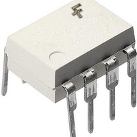
... A maximum input signal of 5mA will provide a minimum output sink current of 13mA (fan out of 8). An internal noise shield provides superior common mode rejection of typically 10kV/µs. The HCPL2601M and HCPL2631M has a minimum CMR of 5kV/µs. The HCPL2611M has a minimum CMR of 10kV/µs. Package Outlines ...
Page 2
... N Fan Out (TTL load) *6.3mA is a guard banded value which allows for at least 20% CTR degradation. Initial input current threshold value is 5.0mA or less. ©2009 Fairchild Semiconductor Corporation 6N137M, HCPL2601M, HCPL2611M, HCPL2630M, HCPL2631M Rev. 1.0 25°C unless otherwise specified) A Parameter Single Channel ...
Page 3
... Delay Time to Output LOW Level |CM | Common Mode H Transient Immunity (at Output HIGH Level) |CM | Common Mode L Transient Immunity (at Output LOW Level) ©2009 Fairchild Semiconductor Corporation 6N137M, HCPL2601M, HCPL2611M, HCPL2630M, HCPL2631M Rev. 1.0 70°C unless otherwise specified) A Test Conditions I = 10mA 25° 10µ 1MHz ...
Page 4
... The maximum tolerable rate of rise of the common mode voltage to ensure the output will remain in the L LOW output state (i.e., V OUT 12. Device considered a two-terminal device: Pins and 4 shorted together, and Pins and 8 shorted together. ©2009 Fairchild Semiconductor Corporation 6N137M, HCPL2601M, HCPL2611M, HCPL2630M, HCPL2631M Rev. 1.0.3 (Continued) = -40 to +85°C unless otherwise specified) Test Conditions V = 5.5V 5.5V, ...
Page 5
... Fig. 5 Input Threshold Current vs. Ambient Temperature 4 3 0. 350Ω 1kΩ 4kΩ L 1.5 1.0 -40 - – AMBIENT TEMPERATURE (°C) A ©2009 Fairchild Semiconductor Corporation 6N137M, HCPL2601M, HCPL2611M, HCPL2630M, HCPL2631M Rev. 1.0 12.8mA 16mA OL 0.100 I = 6.4mA OL 0.010 0.001 100 0 350Ω PLH 4kΩ ...
Page 6
... AMBIENT TEMPERATURE (°C) A Fig. 9 Enable Propagation Delay vs. Temperature 100 I = 7.5mA -40 - – AMBIENT TEMPERATURE (°C) A ©2009 Fairchild Semiconductor Corporation 6N137M, HCPL2601M, HCPL2611M, HCPL2630M, HCPL2631M Rev. 1.0.3 (Continued) 500 400 300 R = 4kΩ L 200 100 R = 1kΩ 350Ω L -100 100 -40 100 ...
Page 7
... Test Circuits Pulse Generator tr = 5ns Input 3 Monitor ( Fig. 12 Test Circuit and Waveforms for t Pulse Generator tr = 5ns 7 ©2009 Fairchild Semiconductor Corporation 6N137M, HCPL2601M, HCPL2611M, HCPL2630M, HCPL2631M Rev. 1.0.3 + bypass Output GND Input Monitor ( + bypass Output GND Fig. 13 Test Circuit t and t EHL 7 ...
Page 8
... Test Circuits (Continued 0.5 V Fig. 14 Test Circuit Common Mode Transient Immunity ©2009 Fairchild Semiconductor Corporation 6N137M, HCPL2601M, HCPL2611M, HCPL2630M, HCPL2631M Rev. 1.0 bypass GND V CM Pulse Gen Peak Switching Pos. (A (Min (Max) O Switching Pos +5V 350 Output ( www.fairchildsemi.com ...
Page 9
... Fairchild products. Always visit Fairchild Semiconductor’s online packaging area for the most recent package drawings: http://www.fairchildsemi.com/packaging/ ©2009 Fairchild Semiconductor Corporation 6N137M, HCPL2601M, HCPL2611M, HCPL2630M, HCPL2631M Rev. 1.0.3 0.4" Lead Spacing (Option TV) (Pending) 0.156 (3.94) 0.144 (3.68) MIN 0 ...
Page 10
... The ‘M’ suffix on the part number is an order identifier only used to identify orders for the white package version. The ‘M’ does not appear on the device’s top mark. ©2009 Fairchild Semiconductor Corporation 6N137M, HCPL2601M, HCPL2611M, HCPL2630M, HCPL2631M Rev. 1.0.3 Standard Through Hole Device, 50 pcs per tube Surface Mount Lead Bend Surface Mount ...
Page 11
... ©2009 Fairchild Semiconductor Corporation 6N137M, HCPL2601M, HCPL2611M, HCPL2630M, HCPL2631M Rev. 1.0 User Direction of Feed Description Tape Width Tape Thickness Sprocket Hole Pitch Sprocket Hole Diameter Sprocket Hole Location Pocket Location Pocket Pitch Pocket Dimensions Cover Tape Width Cover Tape Thickness Max. Component Rotation or Tilt Min ...
Page 12
... Maintained Above (T L Peak Body Package Temperature Time (t ) within 5°C of 260°C P Ramp-down Rate (T Time 25°C to Peak Temperature ©2009 Fairchild Semiconductor Corporation 6N137M, HCPL2601M, HCPL2611M, HCPL2630M, HCPL2631M Rev. 1.0.3 Max. Ramp-up Rate = 3°C/S Max. Ramp-down Rate = 6°C/S Tsmax Preheat Area Tsmin t s 120 240 Time 25° ...
Page 13
... Datasheet Identification Product Status Advance Information Formative / In Design Preliminary First Production No Identification Needed Full Production Obsolete Not In Production ©2009 Fairchild Semiconductor Corporation 6N137M, HCPL2601M, HCPL2611M, HCPL2630M, HCPL2631M Rev. 1.0.3 ® ® PowerTrench SM PowerXS™ Programmable Active Droop ® QFET e-Series QS Quiet Series RapidConfigure Saving our world, 1mW/W/ time™ ...