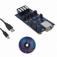
CP2112EK Silicon Laboratories Inc, CP2112EK Datasheet - Page 7

CP2112EK
Manufacturer Part Number
CP2112EK
Description
KIT EVAL FOR CP2112
Manufacturer
Silicon Laboratories Inc
Specifications of CP2112EK
Main Purpose
Interface, USB 2.0 to SMBus Bridge
Embedded
No
Utilized Ic / Part
CP2112
Primary Attributes
Full Speed (12Mbps)
Secondary Attributes
LED Status Indicators
Interface Type
USB
Operating Supply Voltage
3.3 V
Product
Interface Development Tools
For Use With/related Products
CP2112
Lead Free Status / RoHS Status
Lead free / RoHS Compliant
Lead Free Status / RoHS Status
Lead free / RoHS Compliant
Other names
336-2010
Available stocks
Company
Part Number
Manufacturer
Quantity
Price
Company:
Part Number:
CP2112EK
Manufacturer:
Silicon Labs
Quantity:
135
3. Pinout and Package Definitions
*Note: Pins can be left unconnected when not in use.
GPIO.0
GPIO.1
GPIO.2
GPIO.3
GPIO.4
GPIO.5
GPIO.6
GPIO.7
REGIN
Name
VBUS
GND
RST
VPP
SCL
SDA
RXT
CLK
V
TXT
V
D+
D–
DD
IO
Pin #
16*
23*
22*
21*
20*
15*
14*
13*
12*
24
6
5
2
9
7
8
3
4
1
Power Out
Power In
Power In I/O Supply Voltage Input.
Power In 5 V Regulator Input. This pin is the input to the on-chip voltage regulator.
Special
D Out
D Out
D Out
Type
D I/O
D I/O
D I/O
D I/O
D I/O
D I/O
D I/O
D I/O
D I/O
D I/O
D I/O
D I/O
D I/O
D In
Power Supply Voltage Input.
Voltage Regulator Output. See Section 9.
Ground. Must be tied to ground.
Device Reset. Open-drain output of internal POR or V
nal source can initiate a system reset by driving this pin low for the time
specified in Table 4.
VBUS Sense Input. This pin should be connected to the VBUS signal of a
USB network.
Connect a 4.7 µF capacitor between this pin and ground to support ROM
programming via the USB interface.
USB D+
USB D–
Serial Clock signal for SMBus interface.
Serial Data signal for SMBus interface.
This pin is a user-configurable input or output.
In TXT mode, this pin is the Transmit Toggle pin and toggles to indicate
SMBus transmission. The pin is logic high when a transmission is not in
progress.
This pin is a user-configurable input or output.
In RXT mode, this pin is the Receive Toggle pin and toggles to indicate
SMBus transmission. The pin is logic high when a transmission is not in
progress.
This pin is a user-configurable input or output.
This pin is a user-configurable input or output.
This pin is a user-configurable input or output.
This pin is a user-configurable input or output.
This pin is a user-configurable input or output.
This pin is a user-configurable input or output.
In CLK mode, this pin outputs a clock signal whose frequency is configu-
rable.
Table 7. CP2112 Pin Definitions
Rev. 1.0
Description
DD
monitor. An exter-
CP2112
7


