EVB-USB2412 SMSC, EVB-USB2412 Datasheet
EVB-USB2412
Specifications of EVB-USB2412


Related parts for EVB-USB2412


EVB-USB2412 Summary of contents
Page 1
... EVB-USB2412, Revision A1 Evaluation Board Copyright © 2010 SMSC or its subsidiaries. All rights reserved. Circuit diagrams and other information relating to SMSC products are included as a means of illustrating typical applications. Consequently, complete information sufficient for construction purposes is not necessarily given. Although the information has been checked and is believed to be accurate, no responsibility is assumed for inaccuracies. SMSC reserves the right to make changes to specifications and product descriptions at any time without notice ...
Page 2
... USB2412 has been designed to illustrate such an implementation with its outer two layers. Many unpopulated (DNP) sites are incorporated to support optional EMI and ESD support components beyond the minimal BOM for proper function. Revision A1 of the EVB-USB2412 also has an added resistor (R23, 100 Kohms) pull down on NON_REM1 for configuration purposes. Revision 0.2 (02-02-10) ...
Page 3
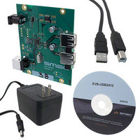
... Connector Description The EVB-USB2412 has a set of standard USB style connectors, one of type B for the upstream port and two of type A for downstream ports. Power is supplied via a 2.1 mm power jack. of the connectors. For more details on the pinout of these connectors, please see the EVB-USB2412 schematics on the CD-ROM included with your EVB-USB2412 ...
Page 4
... Layout Considerations The EVB-USB2412 is designed on four PCB layers--two signal layers and two ground layers. The PCB layer stackup is shown in with ground floods. Internal layers are ground. Note that the differential signals from the USB2412 match the upstream and downstream port placement simplifying the routing of the critical USB signals. ...
Page 5
... PCB routing and ground treatment. The solder side (bottom) layer is shown in Figure 2.2 and ground treatment. Figure 2.1 EVB-USB2412 Top Layer - Component Side SMSC EVB-USB2412 Figure 2.1 to identify the alternate +3.3 Volt regulator location and to illustrate PCB routing ...
Page 6
... Figure 2.2 EVB_USB2412 Bottom Layer - Solder Side Revision 0.2 (02-02-10) EVB-USB2412 Evaluation Board User Manual 6 USER MANUAL SMSC EVB-USB2412 ...