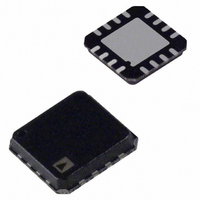
AD8318ACPZ-REEL7 Analog Devices Inc, AD8318ACPZ-REEL7 Datasheet - Page 12

AD8318ACPZ-REEL7
Manufacturer Part Number
AD8318ACPZ-REEL7
Description
IC, LOGARITHMIC AMP, 12NS, LFCSP-16
Manufacturer
Analog Devices Inc
Datasheet
1.AD8318ACPZ-REEL7.pdf
(24 pages)
Specifications of AD8318ACPZ-REEL7
No. Of Amplifiers
1
Dynamic Range, Decades
70
Response Time
12ns
Supply Voltage Range
4.5V To 5.5V
Amplifier Case Style
LFCSP
No. Of Pins
16
Supply Current
68mA
Design Resources
Stable, Closed-Loop Automatic Power Control for RF Appls (CN0050) Software Calibrated, 1 MHz to 8 GHz, 70 dB RF Power Measurement System Using AD8318 (CN0150)
Frequency
1MHz ~ 8GHz
Rf Type
RADAR, 802.11/Wi-Fi, 8.2.16/WiMax, Wireless LAN
Input Range
-60dBm ~ -2dBm
Accuracy
±1dB
Voltage - Supply
4.5 V ~ 5.5 V
Current - Supply
68mA
Package / Case
16-VQFN, CSP Exposed Pad
Rohs Compliant
Yes
Lead Free Status / RoHS Status
Lead free / RoHS Compliant
Other names
AD8318ACPZ-REEL7
AD8318ACPZ-REEL7TR
AD8318ACPZ-REEL7TR
Available stocks
Company
Part Number
Manufacturer
Quantity
Price
Company:
Part Number:
AD8318ACPZ-REEL7
Manufacturer:
FREESCALE
Quantity:
101
AD8318
USING THE AD8318
BASIC CONNECTIONS
The AD8318 is specified for operation up to 8 GHz. As a result,
low impedance supply pins with adequate isolation between
functions are essential. In the AD8318, VPSI and VPSO, the two
positive supply pins, must be connected to the same positive
potential. The VPSI pin biases the input circuitry, while the
VPSO pin biases the low noise output driver for VOUT.
Separate commons are also included in the device. CMOP is
used as the common for the output drivers. Pin CMIP and
Pin CMOP should be connected to a low impedance ground plane.
A power supply voltage of between 4.5 V and 5.5 V should be
applied to VPSO and VPSI. In addition, 100 pF and 0.1 μF
power supply decoupling capacitors connect close to each
power supply pin. The two adjacent VPSI pins can share a pair
of decoupling capacitors due to their proximity.
The paddle of the AD8318 LFCSP is internally connected to
CMIP. For optimum thermal and electrical performance, solder
the paddle to a low impedance ground plane.
ENABLE INTERFACE
To enable the AD8318, the ENBL pin must be pulled high.
Taking ENBL low puts the AD8318 in sleep mode, reducing
current consumption to 260 μA at ambient. The voltage on
ENBL must be greater than 2 V
When enabled, the ENBL pin draws less than 1 μA. When
ENBL is pulled low, the pin sources 15 μA.
The enable interface has high input impedance. An internal
200 Ω resistor is placed in series with the ENBL input for added
protection. Figure 24 depicts a simplified schematic of the
INPUT
1
2
SEE TEMPERATURE COMPENSATION SECTION.
SEE RESPONSE TIME SECTION.
T
EMP
RF
52.3Ω
R1
C1
1nF
C2
1nF
Figure 23. Basic Connections
V
S
13
14
15
16
CMIP
CMIP
TEMP
INHI
INLO
ENBL
12
1
BE
CMIP
CMIP
AD8318
NOTE 1
11
2
(~1.7 V) to enable the device.
499Ω
TADJ
VPSI
V
10
3
S
CMOP
VOUT
VSET
CLPF
VPSO
VPSI
V
9
4
C7
100pF
C8
0.1µF
S
8
7
6
5
C5
0.1µF
C6
100pF
NOTE 2
V
OUT
Rev. B | Page 12 of 24
enable interface. The response time of the AD8318 ENBL
interface is shown in Figure 25.
INPUT SIGNAL COUPLING
The RF input to the AD8318 (INHI) is single ended and must
be ac-coupled. INLO (input common) should be ac-coupled to
ground (see Figure 23). Suggested coupling capacitors are 1 nF
ceramic, 0402-style capacitors for input frequencies of 1 MHz to
8 GHz. The coupling capacitors should be mounted close to the
INHI pin and the INLO pin. These capacitor values can be
increased to lower the input stage high-pass cutoff frequency.
The high-pass corner is set by the input coupling capacitors and
the internal 10 pF capacitor. The dc voltage on INHI and INLO
is approximately one diode voltage drop below the voltage
applied to the VPSI pin.
The Smith Chart in Figure 16 shows the AD8318 input
impedance vs. frequency. Table 4 lists the reflection coefficient
and impedance at select frequencies. For Figure 16 and Table 4,
the 52.3 Ω input termination resistor is removed. At dc, the
resistance is typically 2 kΩ. At frequencies up to 1 GHz, the
impedance is approximated as 1000 Ω||0.7 pF. The RF input
pins are coupled to a network as shown in the simplified
schematic in Figure 26.
1
CH1
500mV
ENBL
CMIP
VPSI
Input AC-Coupling Caps = 18 pF; CLPF = Open
Figure 25. ENBL Response Time; VPOS = 5.0 V;
200Ω
40kΩ
Figure 24. ENBL Interface
40kΩ
M400ns
2 × V
T
BE
425.200ns
2 × V
BE
DISCHARGE
A CH1
ENABLE
920mV
Δ: 2.07V
@: 2.07V


