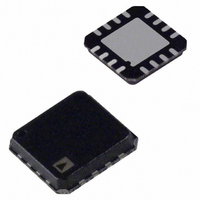
AD8318ACPZ-REEL7 Analog Devices Inc, AD8318ACPZ-REEL7 Datasheet - Page 17

AD8318ACPZ-REEL7
Manufacturer Part Number
AD8318ACPZ-REEL7
Description
IC, LOGARITHMIC AMP, 12NS, LFCSP-16
Manufacturer
Analog Devices Inc
Datasheet
1.AD8318ACPZ-REEL7.pdf
(24 pages)
Specifications of AD8318ACPZ-REEL7
No. Of Amplifiers
1
Dynamic Range, Decades
70
Response Time
12ns
Supply Voltage Range
4.5V To 5.5V
Amplifier Case Style
LFCSP
No. Of Pins
16
Supply Current
68mA
Design Resources
Stable, Closed-Loop Automatic Power Control for RF Appls (CN0050) Software Calibrated, 1 MHz to 8 GHz, 70 dB RF Power Measurement System Using AD8318 (CN0150)
Frequency
1MHz ~ 8GHz
Rf Type
RADAR, 802.11/Wi-Fi, 8.2.16/WiMax, Wireless LAN
Input Range
-60dBm ~ -2dBm
Accuracy
±1dB
Voltage - Supply
4.5 V ~ 5.5 V
Current - Supply
68mA
Package / Case
16-VQFN, CSP Exposed Pad
Rohs Compliant
Yes
Lead Free Status / RoHS Status
Lead free / RoHS Compliant
Other names
AD8318ACPZ-REEL7
AD8318ACPZ-REEL7TR
AD8318ACPZ-REEL7TR
Available stocks
Company
Part Number
Manufacturer
Quantity
Price
Company:
Part Number:
AD8318ACPZ-REEL7
Manufacturer:
FREESCALE
Quantity:
101
VARIATION IN TEMPERATURE DRIFT FROM
DEVICE TO DEVICE
Figure 36 shows a plot of output voltage and error for multiple
AD8318 devices measured at 5.8 GHz. The concentration of
black error plots represents the performance of the population
at 25°C (slope and intercept are calculated for each device).
The red and blue curves indicate the measured behavior of a
population of devices over temperature. This suggests a range
on the drift (from device to device) of 1.2 dB.
Figure 36. Output Voltage and Error vs. Temperature (+25°C, −40°C, and
Figure 35. Error vs. Temperature with Respect to Output Voltage at 25°C
(Does Not Take Transfer Function Nonlinearities at 25°C into Account)
2.2
2.0
1.8
1.6
1.4
1.2
1.0
0.8
0.6
0.4
0.2
2.2
2.0
1.8
1.6
1.4
1.2
1.0
0.8
0.6
0.4
0.2
–65 –60 –55 –50 –45 –40 –35 –30 –25 –20 –15 –10 –5
–65
+85°C) of a Population of Devices Measured at 5.8 GHz
–55
V
V
V
–45
OUT
OUT
OUT
+25°C
–40°C
+85°C
–35
P
P
IN
IN
–25
ERROR +25°C wrt V
ERROR –40°C wrt V
ERROR +85°C wrt V
(dBm)
(dBm)
–15
–5
OUT
OUT
OUT
5
0
15
5
2.5
2.0
1.5
1.0
0.5
0
–0.5
–1.0
–1.5
–2.0
–2.5
2.0
1.6
1.2
0.8
0.4
0
–0.4
–0.8
–1.2
–1.6
–2.0
Rev. B | Page 17 of 24
TEMPERATURE DRIFT AT DIFFERENT
TEMPERATURES
Figure 37 shows the log slope and error over temperature for
a 5.8 GHz input signal. Error due to drift over temperature
consistently remains within ±0.5 dB, and only begins to exceed
this limit when the ambient temperature drops below −20°C.
When using a reduced temperature range, higher measurement
accuracy is achievable for all frequencies.
SETTING THE OUTPUT SLOPE IN MEASUREMENT
MODE
To operate in measurement mode, VOUT is connected to VSET.
This yields the typical logarithmic slope of −25 mV/dB. The
output swing corresponding to the specified input range is then
approximately 0.5 V to 2.1 V. The slope and output swing can be
increased by placing a resistor divider between VOUT and
VSET (that is, one resistor from VOUT to VSET and one
resistor from VSET to common).
As an example, if two equal resistors, such as 10 kΩ/10 kΩ, are
used, the slope doubles to approximately −50 mV/dB. The input
impedance of VSET is approximately 500 kΩ. Slope setting
resistors should be kept below ~50 kΩ to prevent this input
impedance from affecting the resulting slope. When increasing
the slope, the new output voltage range cannot exceed the
output voltage swing capability of the output stage. Refer to the
Measurement Mode section for further details.
2.2
2.0
1.8
1.6
1.4
1.2
1.0
0.8
0.6
0.4
0.2
–65 –60 –55 –50 –45 –40 –35 –30 –25 –20 –15 –10 –5
Figure 37. Typical Drift at 5.8 GHz for Various Temperatures
V
V
ERROR –10°C
ERROR +70°C
OUT
OUT
+25°C
0°C
Figure 38. Increasing the Slope
AD8318
VOUT
VSET
P
IN
V
V
ERROR –20°C
V
ERROR –40°C
(dBm)
OUT
OUT
OUT
–40°C
+70°C
–10°C
10kΩ
10kΩ
–50mV/dB
V
ERROR +25°C
ERROR 0°C
V
ERROR +85°C
OUT
OUT
+85°C
–20°C
0
AD8318
5
2.5
2.0
1.5
1.0
0.5
0
–0.5
–1.0
–1.5
–2.0
–2.5


