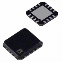
AD8318ACPZ-REEL7 Analog Devices Inc, AD8318ACPZ-REEL7 Datasheet - Page 18

AD8318ACPZ-REEL7
Manufacturer Part Number
AD8318ACPZ-REEL7
Description
IC, LOGARITHMIC AMP, 12NS, LFCSP-16
Manufacturer
Analog Devices Inc
Datasheet
1.AD8318ACPZ-REEL7.pdf
(24 pages)
Specifications of AD8318ACPZ-REEL7
No. Of Amplifiers
1
Dynamic Range, Decades
70
Response Time
12ns
Supply Voltage Range
4.5V To 5.5V
Amplifier Case Style
LFCSP
No. Of Pins
16
Supply Current
68mA
Design Resources
Stable, Closed-Loop Automatic Power Control for RF Appls (CN0050) Software Calibrated, 1 MHz to 8 GHz, 70 dB RF Power Measurement System Using AD8318 (CN0150)
Frequency
1MHz ~ 8GHz
Rf Type
RADAR, 802.11/Wi-Fi, 8.2.16/WiMax, Wireless LAN
Input Range
-60dBm ~ -2dBm
Accuracy
±1dB
Voltage - Supply
4.5 V ~ 5.5 V
Current - Supply
68mA
Package / Case
16-VQFN, CSP Exposed Pad
Rohs Compliant
Yes
Lead Free Status / RoHS Status
Lead free / RoHS Compliant
Other names
AD8318ACPZ-REEL7
AD8318ACPZ-REEL7TR
AD8318ACPZ-REEL7TR
Available stocks
Company
Part Number
Manufacturer
Quantity
Price
Company:
Part Number:
AD8318ACPZ-REEL7
Manufacturer:
FREESCALE
Quantity:
101
AD8318
RESPONSE TIME CAPABILITY
The AD8318 has a 10 ns rise/fall time capability (10% to 90%)
for input power switching between the noise floor and 0 dBm.
This capability enables RF burst measurements at repetition
rates beyond 45 MHz. In most measurement applications, the
AD8318 has an external capacitor connected to CLPF to
provide additional filtering for VOUT. However, using the
CLPF capacitor slows the response time as does stray capacitance
on VOUT. For an application requiring maximum RF burst
detection capability, the CLPF pin is left unconnected. In this
case, the integration function is provided by the 1.5 pF on-chip
capacitor.
There is a 10 Ω internal resistor in series with the output driver.
Because of this resistor, it is necessary to add an external 40 Ω
back-terminating resistor in series with the output when driving
a 50 Ω load. Place the back-terminating resistor close to the
VOUT pin. The AD8318 has the drive capability to drive a 50 Ω
load at the end of a coaxial cable or transmission line when back
terminated (see Figure 39).
The circuit diagram in Figure 39 shows the AD8318 used with a
high speed comparator circuit. The 40 Ω series resistor at the
output of the AD8318 combines with an internal 10 Ω to
properly match to the 50 Ω input of the comparator.
0
PULSED RF
AD8318
OUTPUT
COMPARATOR
OUTPUT
Figure 40. Pulse Response of AD8318 and Comparator for RF Pulses
INPUT
100
–50dB
200
300
of Varying Amplitudes
–30dB
PULSED RF
TIME (ns)
INPUT
400
–20dB
1nF
1nF
500
Figure 39. AD8318 Operating with the High Speed ADCMP563 Comparator
52.3Ω
600
–10dB
INHI
INLO
AD8318
VPOS
GND
+5V
700
VOUT
VSET
V
REF
800
= 1.8V–1.2V
Rev. B | Page 18 of 24
50Ω
40Ω
OUTPUT
AD8318
50Ω
Figure 40 shows the response of the AD8318 and the comparator
for a 500 MHz pulsed sine wave of varying amplitudes. The
output level of the AD8318 is the signal strength of the input
signal. For applications where these RF bursts are very small,
the output level does not change by a large amount. Using a
comparator is beneficial in this case because it turns the output
of the log amp into a limiter-like signal. While this configuration
does result in the loss of received signal power level, it does
allow for presence-only detection of low power RF bursts.
OUTPUT FILTERING
For applications in which maximum video bandwidth and,
consequently, fast rise time are desired, it is essential that the
CLPF pin be left unconnected and free of any stray capacitance.
To reduce the nominal output video bandwidth of 45 MHz,
connect a ground-referenced capacitor (C
as shown in Figure 41. Generally, this is done to reduce output
ripple (at twice the input frequency for a symmetric input
waveform, such as sinusoidal signals).
C
Set the video bandwidth to a frequency equal to about one-
tenth the minimum input frequency. This ensures that the
output ripple of the demodulated log output, which is at twice
the input frequency, is well filtered.
ADCMP563
FLT
–5.2V
+5V
is selected by
C
FLT
100Ω
Figure 41. Lowering the Postdemodulation Bandwidth
–5.2V
=
(
π
I
3.13kΩ
LOG
×
100Ω
3.13
50Ω
50Ω
kΩ
×
COMPARATOR
1.5pF
VideoBandw
1
OUTPUT
AD8318
+4
idth
FLT
VOUT
CLPF
)
) to the CLPF pin,
−
1
C
5 .
FLT
pF
(19)


