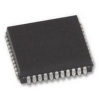
MM5452V National Semiconductor, MM5452V Datasheet - Page 4

MM5452V
Manufacturer Part Number
MM5452V
Description
LCD DISPLAY DRIVER, 5452, PLCC44
Manufacturer
National Semiconductor
Datasheet
1.MM5452V.pdf
(9 pages)
Specifications of MM5452V
Module Configuration
CMOS
Supply Current
40µA
No. Of Segments
32
Meter Display Type
LCD
Supply Voltage Range
3V To 10V
Driver Case Style
LCC
No. Of Pins
44
Operating Temperature Range
-40°C To
No. Of Digits / Alpha
4.1/2
Rohs Compliant
Yes
Lead Free Status / RoHS Status
Lead free / RoHS Compliant
Available stocks
Company
Part Number
Manufacturer
Quantity
Price
Company:
Part Number:
MM5452V
Manufacturer:
national
Quantity:
1
Part Number:
MM5452V
Manufacturer:
NS
Quantity:
20 000
Company:
Part Number:
MM5452V/NOPB
Manufacturer:
Texas Instruments
Quantity:
10 000
Part Number:
MM5452VX
Manufacturer:
NS/国半
Quantity:
20 000
Company:
Part Number:
MM5452VX/NOPB
Manufacturer:
Texas Instruments
Quantity:
10 000
www.national.com
Functional Description
The MM5452 is specifically designed to operate 4
7-segment displays with minimal interface with the display
and the data source. Serial data transfer from the data
source to the display driver is accomplished with 2 signals,
serial data and clock. Since the MM5452 does not contain a
character generator, the formatting of the segment informa-
tion must be done prior to inputting the data to the MM5452.
Using a format of a leading “1” followed by the 32 data bits
allows data transfer without an additional load signal. The 32
data bits are latched after the 36th clock is complete, thus
providing non-multiplexed, direct drive to the display. Out-
puts change only if the serial data bits differ from the previ-
ous time.
A block diagram is shown in Figure 1 . For the MM5452 a
DATA ENABLE is used instead of the 33rd output. If the
DATA ENABLE signal is not required, the 33rd output can be
brought out. This is the MM5453 device.
Figure 6 shows a typical application. Note how the input data
maps to the output pins and the display. The MM5452 and
MM5453 do not have format restrictions, as all outputs are
FIGURE 5. Input Data Format
1
⁄
2
-digit
FIGURE 4.
4
Figure 5 shows the input data format. A start bit of logical “1”
precedes the 32 bits of data. At the 36th clock a LOAD signal
is generated synchronously with the high state of the clock,
which loads the 32 bits of the shift registers into the latches.
At the low state of the clock a RESET signal is generated
which clears all the shift registers for the next set of data.
The shift registers are static master-slave configuration.
There is no clear for the master portion of the first shift
register, thus allowing continuous operation.
If the clock is not continuous, there must be a complete set
of 36 clocks otherwise the shift registers will not clear.
Figure 2 shows the pin-out of the MM5452. Bit 1 is the first
bit following the start bit and it will appear on pin 18.
Figure 4 shows the timing relationships between data, clock
and DATA ENABLE.
controllable. The application assumes a specific display
pinout. Different display/driver connection patterns will, of
course, yield a different input data format.
00613704
00613705


