DS14C335MSA National Semiconductor, DS14C335MSA Datasheet
DS14C335MSA
Specifications of DS14C335MSA
Available stocks


Related parts for DS14C335MSA


DS14C335MSA Summary of contents
Page 1
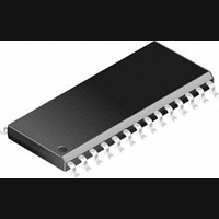
... Small Outline Packaging (SSOP). This device’s low power requirement and small footprint makes it an ideal choice for Laptop and Notebook applica- tions. Connection Diagram DS14C335 Order Number DS14C335MSA See NS Package Number MSA28 Lap-Link ® registered trademark of Traveling Software. © 2004 National Semiconductor Corporation Features n Conforms to TIA/EIA-232-E and CCITT V ...
Page 2
... Absolute Maximum Ratings If Military/Aerospace specified devices are required, please contact the National Semiconductor Sales Office/ Distributors for availability and specifications. Supply Voltage ( Pin − V Pin Input Voltage (DIN, SD) Driver Output Voltage Receiver Input Voltage Receiver Output Voltage Junction Temperature Storage Temperature Range Lead Temperature (Soldering 4 sec ...
Page 3
Electrical Characteristics Over recommended operating conditions 0.8V, unless otherwise specified. Symbol Parameter RECEIVER CHARACTERISTICS (Note 4) V Hysteresis HY R Input Resistance IN I Input Current IN V High Level Output OH Voltage V Low Level Output Voltage ...
Page 4
Parameter Measurement Information FIGURE 1. Driver Propagation Delay and Slew Rate Test Circuit FIGURE 2. Driver Propagation Delay and Slew Rate Timing FIGURE 5. Driver SHUTDOWN (SD) Delay Test Circuit www.national.com FIGURE 3. Receiver Propagation Delay Test Circuit FIGURE 4. ...
Page 5
Parameter Measurement Information FIGURE 6. Driver SHUTDOWN (SD) Delay Timing FIGURE 7. Receiver SHUTDOWN (SD) Delay Test Circuit FIGURE 8. Receiver SHUTDOWN (SD) Delay Timing Pin Descriptions V (Pin 3). Power supply pin for the device, +3. ...
Page 6
Pin Descriptions (Continued) R 1–5 (Pins 19, 18, 17, 16, 15). Receiver input pins accept IN ± TIA/EIA-232-E input voltages ( 25V). Receivers guarantees hysteresis of TBD mV. Unused receiver input pins may be left open. Internal input resistor (5 ...
Page 7
Application Information vertor also provides a larger signal swing (higher at RS-232 standard data rates) which translates to more noise margin for the rejection of ground potential differences, induced noise, and crosstalk compared to other DC-DC convertor schemes which only ...
Page 8
Typical Performance Characteristics Driver Output vs Data Rate www.national.com (Continued) 01173416 8 ...
Page 9
... National does not assume any responsibility for use of any circuitry described, no circuit patent licenses are implied and National reserves the right at any time without notice to change said circuitry and specifications. inches (millimeters) unless otherwise noted Order Number DS14C335MSA NS Package Number MSA28 2 ...