DS14C535MSA National Semiconductor, DS14C535MSA Datasheet

IC, RS-232 TRANSCEIVER, 5.5V, SSOP-28

DS14C535MSA

Manufacturer Part Number
DS14C535MSA
Description
IC, RS-232 TRANSCEIVER, 5.5V, SSOP-28
Manufacturer
National Semiconductor
Datasheet

Specifications of DS14C535MSA

Device Type
Driver / Receiver
Ic Interface Type
RS232
No. Of Drivers
3
Supply Voltage Range
4.5V To 5.5V
Driver Case Style
SSOP
No. Of Pins
28
Operating Temperature Range
0°C To +70°C
Lead Free Status / RoHS Status
Contains lead / RoHS non-compliant

Available stocks

Company
Part Number
Manufacturer
Quantity
Price
Part Number:
DS14C535MSA
Manufacturer:
NSC
Quantity:
8 000
Part Number:
DS14C535MSA
Manufacturer:
NS/国半
Quantity:
20 000
Part Number:
DS14C535MSAX
Manufacturer:
NS
Quantity:
10 000
Part Number:
DS14C535MSAX
Manufacturer:
NS/国半
Quantity:
20 000
Company:
Part Number:
DS14C535MSAX
Quantity:
911
Part Number:
DS14C535MSAX/NOPB
Manufacturer:
MAXIM/美信
Quantity:
20 000
© 2004 National Semiconductor Corporation
DS14C535
+5V Supply EIA/TIA-232 3 x 5 Driver/Receiver
General Description
The DS14C535 is three driver, five receiver device which
conforms to EIA/TIA-232-E and CCITT (ITU-T) V.28 stan-
dard specifications. This device employs an internal DC-DC
converter to generate the necessary output levels from a
+5V power supply. A SHUTDOWN (SD) mode reduces the
supply current to 10 µA maximum. In the SD mode, one
receiver is active, allowing ring indicator (RI) to be moni-
tored. PC Board space consumption is minimized by the
availability of Shrink Small Outline Packaging (SSOP).
The DS14C535 provides a one-chip solution for the common
9-pin serial RS-232 interface between data terminal and
data circuit-terminating equipment.
This device allows an easy migration path to the 3.3V
DS14C335. The packages are the same. The N/C pins on
the DS14C535 are not physically connected to the chip.
Board layout for the DS14C335 will accommodate both de-
vices.
This device’s low power requirement and small footprint
makes it an ideal choice for Laptop and Notebook applica-
tions.
Connection Diagram
Lap-Link
®
is a registered trademark of Traveling Software Inc.
See NS Package Number MSA28
Order Number DS14C535MSA
DS14C535
DS011910
01191001
Features
n Pin compatible with DS14C335
n Conforms to EIA/TIA-232-E and CCITT (ITU-T) V.28
n Failsafe receiver outputs high when inputs open
n Operates with single +5V power supply
n Low power requirement — I
n SHUTDOWN mode — I
n One Receiver (R5) active during SHUTDOWN
n Operates up to 128 kbps — Lap-Link
n 4V/µs minimum Slew Rate guaranteed
n ESD rating of 3 kV on all pins (H, B, M)
n Available in 28-lead SSOP EIAJ Type II package
n Only four 0.1 µF capacitors required for the DC-DC
Functional Diagram
specifications
converter
CX
10 µA maximum
CC
12 mA maximum
®
Compatible
01191002
www.national.com
May 1998

Related parts for DS14C535MSA

DS14C535MSA Summary of contents

Page 1

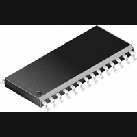
... This device’s low power requirement and small footprint makes it an ideal choice for Laptop and Notebook applica- tions. Connection Diagram DS14C535 Order Number DS14C535MSA See NS Package Number MSA28 Lap-Link ® registered trademark of Traveling Software Inc. © 2004 National Semiconductor Corporation ...

Page 2

... Absolute Maximum Ratings If Military/Aerospace specified devices are required, please contact the National Semiconductor Sales Office/ Distributors for availability and specifications. Supply Voltage ( Pin − V Pin Input Voltage (D , SD) IN Driver Output Voltage Receiver Input Voltage Receiver Output Voltage Junction Temperature Storage Temperature Range Lead Temperature (Soldering 4 sec ...

Page 3

Electrical Characteristics Over recommended operating conditions 0.8V, unless otherwise specified. Symbol Parameter DRIVER CHARACTERISTICS I Input Current IN V High Level Output Voltage OH V Low Level Output Voltage OL Switching Characteristics Over recommended operating conditions ...

Page 4

Parameter Measurement Information FIGURE 2. Driver Propagation Delay and Slew Rate Timing FIGURE 5. Driver SHUTDOWN (SD) Delay Test Circuit www.national.com (Continued) FIGURE 3. Receiver Propagation Delay Test Circuit FIGURE 4. Receiver Propagation Delay Timing 4 01191004 01191005 01191006 01191007 ...

Page 5

Parameter Measurement Information FIGURE 6. Driver SHUTDOWN (SD) Delay Timing FIGURE 7. Receiver SHUTDOWN (SD) Delay Test Circuit FIGURE 8. Receiver SHUTDOWN (SD) Delay Timing Pin Descriptions V (Pin 3). Power supply pin for the device, + ...

Page 6

Application Information is in SHUTDOWN (SD) mode, receiver five (R5) remains active and monitors RI circuit. This active receiver (R5) alerts the DTE to switch the DS14C535 from SHUTDOWN to active mode. www.national.com To achieve minimum power consumption, the DS14C535 ...

Page 7

Application Information CAPACITORS Capacitors can be ceramic or tantalum. Standard surface mount in the range of 0.1 µF to 0.68 µF are readily available from several manufacturers. A minimum 20V rating is rec- ommended. Contact manufacturers for specific detail on ...

Page 8

... National does not assume any responsibility for use of any circuitry described, no circuit patent licenses are implied and National reserves the right at any time without notice to change said circuitry and specifications. inches (millimeters) unless otherwise noted Order Number DS14C535MSA NS Package Number MSA28 2 ...

Related keywords